Semiconductor system assemblies and methods of operation

a technology of semiconductors and components, applied in the direction of electrical equipment, basic electric elements, electric discharge tubes, etc., can solve the problems of deformation of remaining materials, deformation of local plasmas, and difficulty in penetrating wet processes, so as to improve plasma control, prevent electrode and other chamber components from degrading, and improve etching profiles

Inactive Publication Date: 2015-06-18
APPLIED MATERIALS INC
View PDF0 Cites 180 Cited by
  • Summary
  • Abstract
  • Description
  • Claims
  • Application Information

AI Technical Summary

Benefits of technology

[0011]Such technology may provide numerous benefits over conventional systems and techniques. For example, degradation of the electrode and other chamber components may be prevented or limited. An additional advantage is that improved e

Problems solved by technology

However, wet processes may have difficulty penetrating some constrained trenches and also may sometimes deform the remai

Method used


Image

  • Semiconductor system assemblies and methods of operation
  • Semiconductor system assemblies and methods of operation
  • Semiconductor system assemblies and methods of operation

Examples


Embodiment Construction

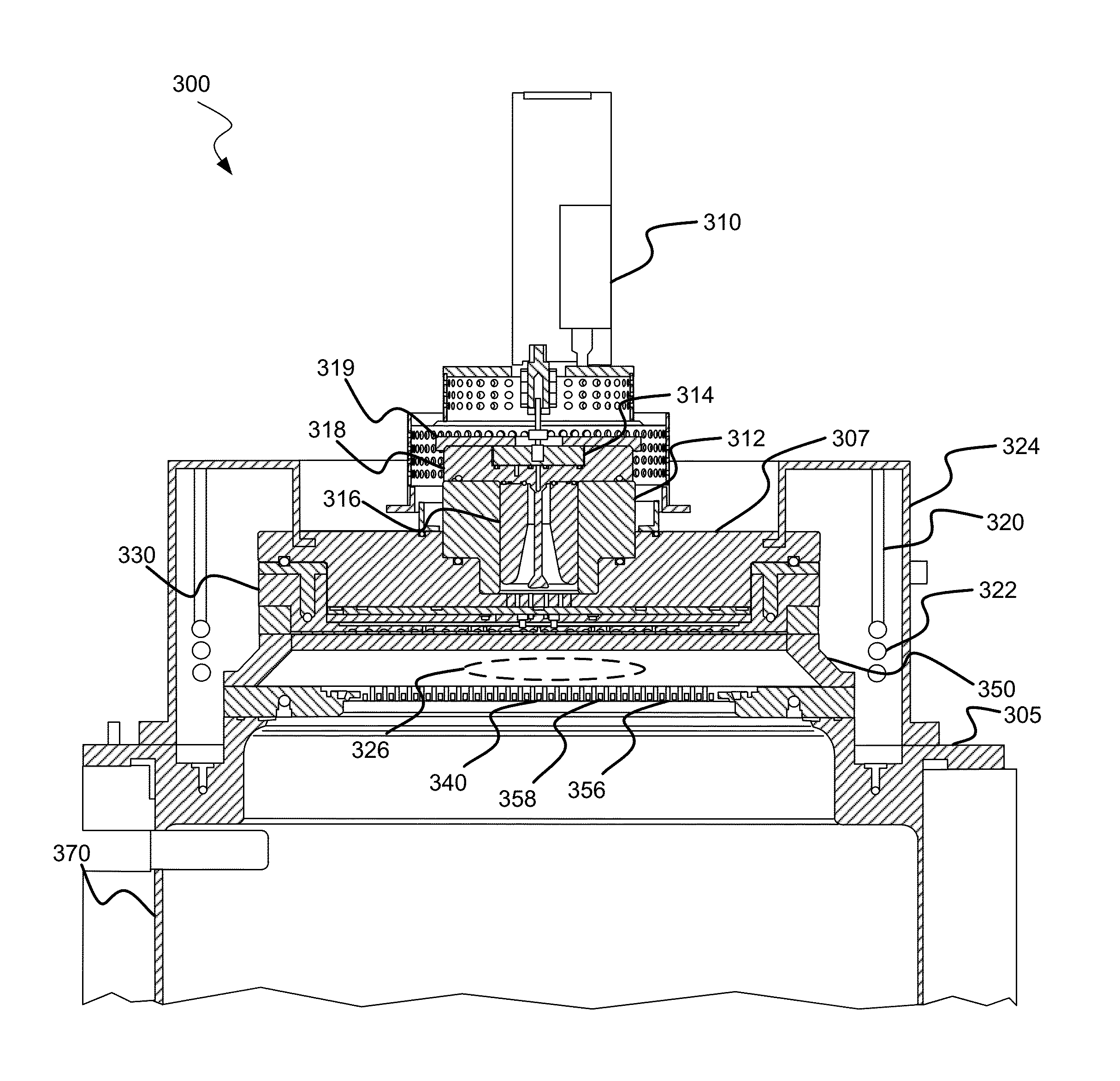
[0025]The present technology includes systems and components for semiconductor processing. When plasmas are formed in situ in processing chambers, such as with a capacitively coupled plasma (“CCP”) for example, exposed surfaces of the chamber may be sputtered or degraded by the plasma or the species produced by the plasma. This may in part be caused by bombardment to the surfaces or surface coatings by generated plasma particles. The extent of the bombardment may itself be related to the voltage utilized in generating the plasma. For example, higher voltage may cause higher bombardment, and further degradation.

[0026]Conventional technologies have often dealt with this degradation by providing replaceable components within the chamber. Accordingly, when coatings or components themselves are degraded, the component may be removed and replaced with a new component that will in turn degrade over time. By utilizing configurations in which plasma is formed externally to the chamber, or in...


PUM

PropertyMeasurementUnit
Angleaaaaaaaaaa
Frequencyaaaaaaaaaa
Plasma poweraaaaaaaaaa

Abstract

An exemplary semiconductor processing system may include a processing chamber and a first plasma source. The first plasma source may utilize a first electrode positioned externally to the processing chamber, and the first plasma source may be configured to generate a first plasma. The processing system may further comprise a second plasma source separate from the first plasma source that utilizes a second electrode separate from the first electrode. The second electrode may be positioned externally to the processing chamber, and the second plasma source may be configured to generate a second plasma within the processing chamber. The processing system may further comprise a showerhead disposed between the relative locations of the first plasma electrode and the second plasma electrode.

Description

CROSS-REFERENCES TO RELATED APPLICATIONS[0001]This application is related to U.S. application Ser. No. ______ (Attorney Docket No. 80042-890135 (114800US)) entitled “SEMICONDUCTOR SYSTEM ASSEMBLIES AND METHODS OF OPERATION,” and U.S. application Ser. No. ______ (Attorney Docket No. 80042-894190 (114801US)) entitled “SEMICONDUCTOR SYSTEM ASSEMBLIES AND METHODS OF OPERATION,” all of which being filed concurrently on Dec. 17, 2013, the entire disclosures of which are hereby incorporated by reference for all purposes.TECHNICAL FIELD[0002]The present technology relates to semiconductor systems, processes, and equipment. More specifically, the present technology relates to systems and methods for reducing film contamination and equipment degradation.BACKGROUND[0003]Integrated circuits are made possible by processes which produce intricately patterned material layers on substrate surfaces. Producing patterned material on a substrate requires controlled methods for removal of exposed materi...

Claims


Application Information

Patent Timeline
IPC IPC(8): H01L21/67H01L21/3065
CPCH01L21/3065H01L21/67069H01J37/32082H01J37/32091H01J37/321H01J37/32357H01J37/3244
Inventor NGUYEN, ANDREWRAMASWAMY, KARTIKNEMANI, SRINIVASHOWARD, BRADLEYVISHWANATH, YOGANANADA SARODE
Owner APPLIED MATERIALS INC
Why Eureka
Try Eureka