Using dynamic bursts to support frequency-agile memory interfaces

a technology of frequency-agile memory and dynamic bursts, applied in the field of clock memory systems, can solve the problems of not being able to take full advantage of these speed and voltage reductions

Active Publication Date: 2015-06-25
RAMBUS INC
View PDF5 Cites 1 Cited by
  • Summary
  • Abstract
  • Description
  • Claims
  • Application Information

AI Technical Summary

Benefits of technology

The patent text describes a method and apparatus for reducing power consumption in a link circuitry between a processor and a memory device in a portable computing device. The invention uses a clocked memory system that supports dynamic bursts to facilitate agile communication between the processor and memory device at varying data loads and improves power efficiency. The technical effect of the invention is to reduce power consumption in the link circuitry while the processor enters a power-saving mode, resulting in improved battery life for the portable computing device.

Problems solved by technology

However, link interface circuitry between the processor and the memory as well as analog / mixed-mode circuitry is typically not implemented exclusively in rail-to-rail CMOS and consequently cannot always take full advantage of these speed and voltage reductions.

Method used


Image

  • Using dynamic bursts to support frequency-agile memory interfaces
  • Using dynamic bursts to support frequency-agile memory interfaces
  • Using dynamic bursts to support frequency-agile memory interfaces

Examples


Embodiment Construction

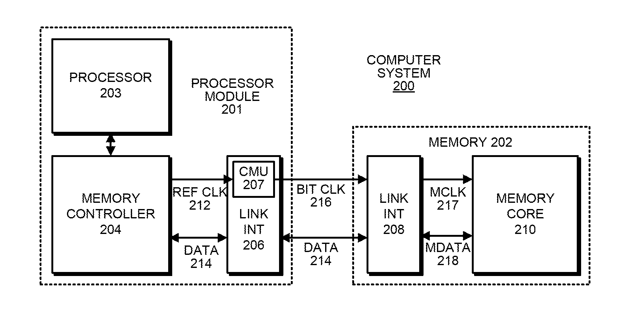
[0017]As mentioned previously, during a power-saving mode it is desirable to reduce power consumption in the link circuitry which connects the processor and the memory. For example, the graph presented in FIG. 1 illustrates power consumption 102 for a link (in mW) and also energy consumed per bit transferred 104 (in mW / Gbps) as a function of the data rate. In this graph, the horizontal axis is associated with data rate (in Gbps) and the vertical axis is associated with power (in mW) and energy consumption per bit (in mW / Gbps). Note that as the data rate increases, power consumption 102 also increases. In contrast, as data rate increases, the energy consumed per bit 104 actually decreases until a sweet spot 106 is reached. This decrease in energy consumed per bit 104 is due to the fact that at lower data rates certain portions of the link circuitry continue to consume constant power whether the link is transmitting data or not, so energy consumption per bit 104 actually increases. (F...


PUM


Abstract

The disclosed embodiments relate to a system that supports dynamic bursts to facilitate frequency-agile communication between a START memory controller and a memory device. During operation, the system monitors a reference clock signal received at an interface between the memory device and the memory controller. Upon detecting a frequency change in the reference clock signal from a fullrate to a subrate, the interface operates in a burst mode, wherein data is communicated through bursts separated by intervening low-power intervals during which portions of the interface are powered down.

Description

BACKGROUND[0001]1. Field[0002]The disclosed embodiments generally relate to clocked memory systems. More specifically, the disclosed embodiments relate to a clocked memory system that supports dynamic bursts to facilitate agile communication between a memory controller and a memory device at varying data loads and improved power efficiency.[0003]2. Related Art[0004]A portable computing device typically enters a power-saving mode to operate at reduced clock speeds when computational workloads are low. These reduced clock speeds enable the supply voltage to be reduced for rail-to-rail Complementary Metal-Oxide-Semiconductor (CMOS) circuits in the portable computing device, which reduces power consumption and thereby extends battery life. However, link interface circuitry between the processor and the memory as well as analog / mixed-mode circuitry is typically not implemented exclusively in rail-to-rail CMOS and consequently cannot always take full advantage of these speed and voltage r...

Claims


Application Information

Patent Timeline
IPC IPC(8): G06F1/32
CPCG06F1/324G06F1/3237G06F13/1689G06F1/3287G06F13/1673G06F13/28Y02D10/00Y02D30/50
InventorZERBE, JARED L.TSANG, BRIAN HING-KITDALY, BARRY WILLIAM
OwnerRAMBUS INC