Semiconductor device and method of manufacturing the same

a semiconductor and semiconductor technology, applied in the field of semiconductor devices, can solve the problems of physical limits in increasing the degree of integration of memory cells, difficult manufacturing processes, and two-dimensional memory devices in which memory cells are fabricated, and achieve the effect of simplifying manufacturing processes and stabilizing structur

Active Publication Date: 2015-06-25
SK HYNIX INC
View PDF2 Cites 344 Cited by
  • Summary
  • Abstract
  • Description
  • Claims
  • Application Information

AI Technical Summary

Benefits of technology

[0008]Exemplary embodiments of the present invention are directed to a semiconductor device having simplified manufacturing processes and a stabilized structure, and a method of manufacturing the same.

Problems solved by technology

Two-dimensional memory devices in which memory cells are fabricated in a single layer over a silicon substrate have reached physical limits in increasing their degree of integration.
However, since contact plugs need to be formed at various depths to realize the 3D non-volatile memory device configured as described above, manufacturing processes may be difficult to perform.

Method used


Image

  • Semiconductor device and method of manufacturing the same
  • Semiconductor device and method of manufacturing the same
  • Semiconductor device and method of manufacturing the same

Examples


Embodiment Construction

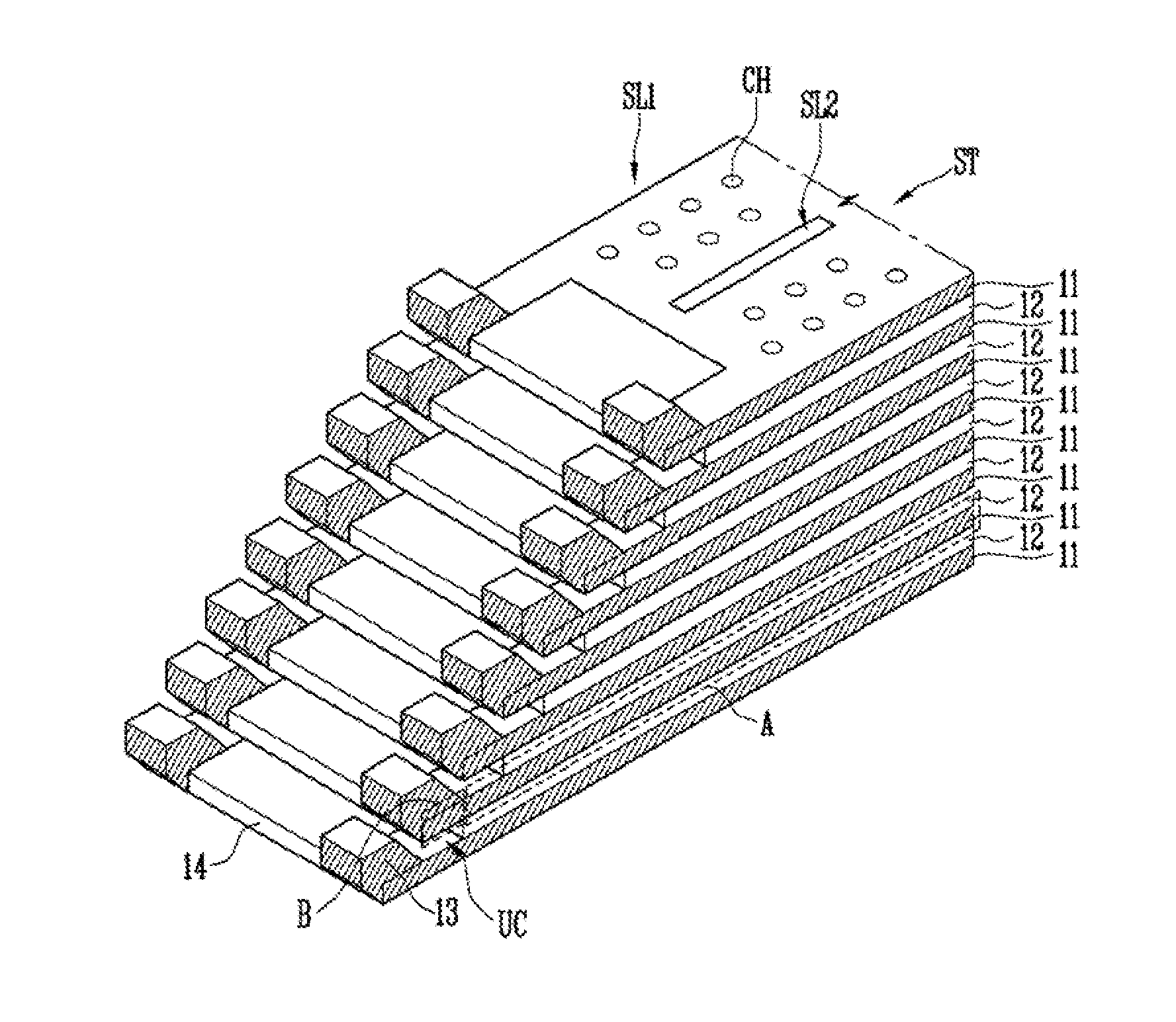
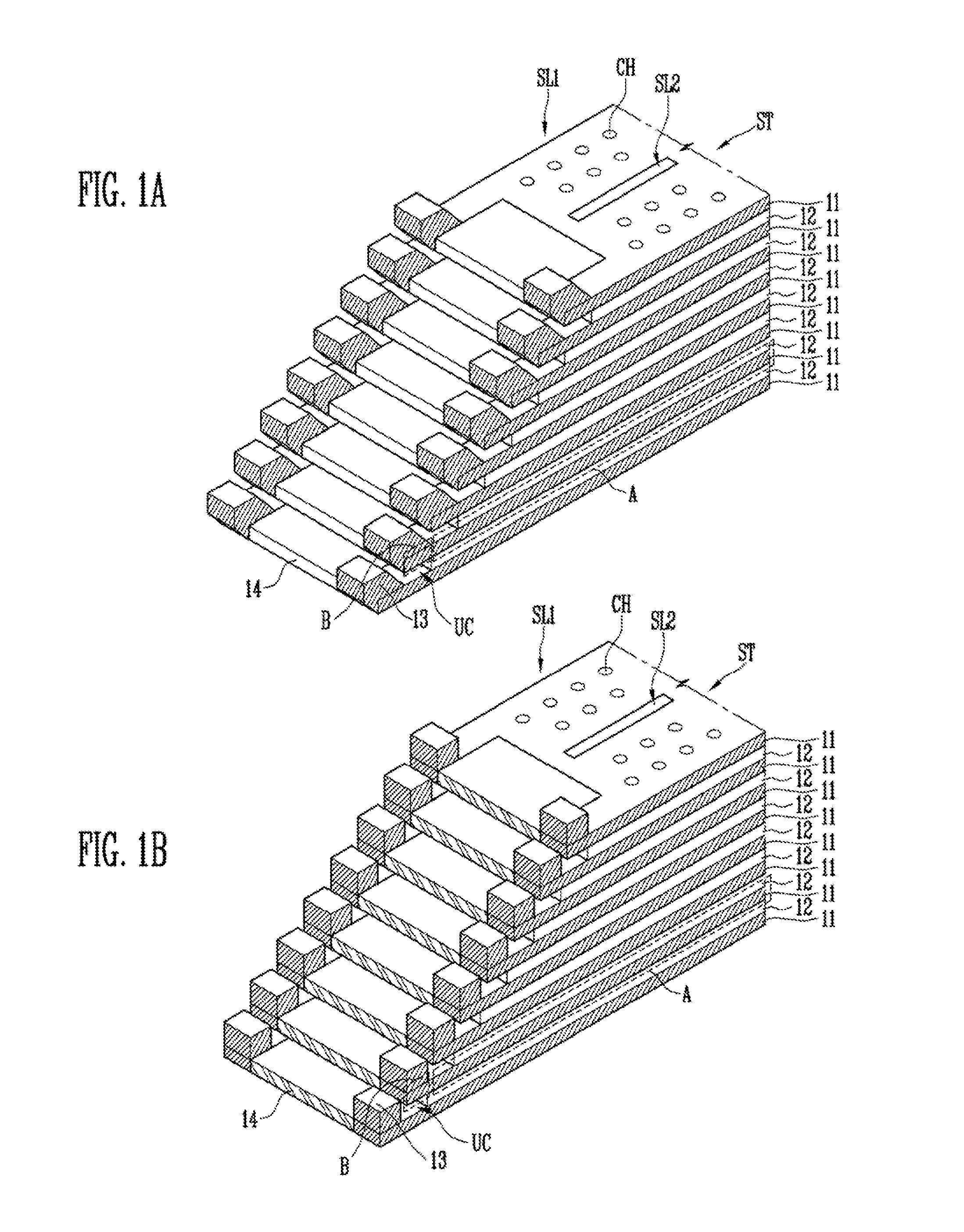
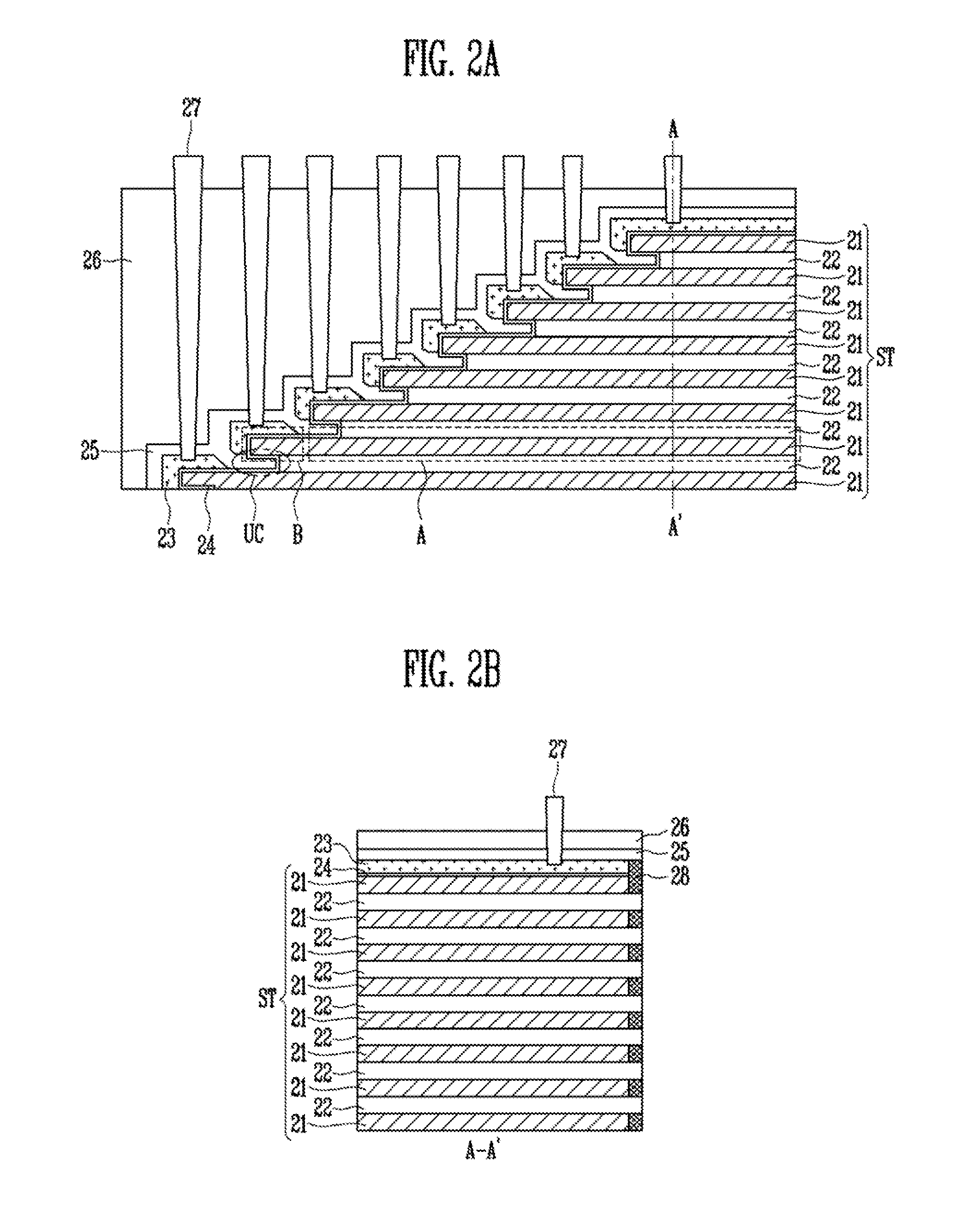
[0022]Various embodiments of the present disclosure will be described in detail with reference to the accompanying drawings. The present invention may, however, be embodied in different forms and should not be construed as limited to the embodiments set forth herein. Rather, these embodiments are provided so that this disclosure will be thorough and complete, and will fully convey the scope of the present invention to those skilled in the art. In the drawings, the thicknesses and length of components are exaggerated for convenience of illustration. In the following description, a detailed explanation of known related functions and constitutions may be omitted to avoid unnecessarily obscuring the subject matter of the present invention. Like reference numerals refer to like elements throughout the specification and drawings.

[0023]Furthermore, ‘connected / coupled’ represents that one component is directly coupled to another component or indirectly coupled through another component, pos...


PUM


Abstract

A semiconductor device includes a stacked structure having first conductive layers stacked stepwise and first insulating layers interposed between the first conductive layers, wherein undercuts are formed under the first conductive layers and each of the first conductive layers includes a first region covered by the first conductive layer and a second region extending from the first region, contact pads coupled to the second regions of the respective first conductive layers, and a liner layer formed on the contact pads and filling the undercuts.

Description

CROSS-REFERENCE TO RELATED APPLICATION[0001]The present application claims priority to Korean patent application number 10-2013-0160219, filed on Dec. 20, 2013, the entire disclosure of which is incorporated herein in its entirety by reference.BACKGROUND[0002]1. Field of Invention[0003]Various exemplary embodiments of the present invention relate generally to an electronic device, and more particularly, to a semiconductor device and a method of manufacturing the same.[0004]2. Description of Related Art[0005]A non-volatile memory device preserves the stored data even when the power is cut off. Two-dimensional memory devices in which memory cells are fabricated in a single layer over a silicon substrate have reached physical limits in increasing their degree of integration. Accordingly, three-dimensional (3D) non-volatile memory devices in which memory cells are stacked in a direction perpendicular to a silicon substrate have been proposed.[0006]A 3D non-volatile memory device may inc...

Claims


Application Information

Patent Timeline
Patent Type & Authority Applications(United States)
IPC IPC(8): H01L23/528H01L27/105H01L23/532
CPCH01L23/528H01L27/1052H01L23/53271H01L2924/0002H10B41/50H10B41/27H10B43/50H10B43/27H01L2924/00H01L21/28H10B69/00H10B99/00H01L23/5226
Inventor LEE, KI HONGPYI, SEUNG HOBAEK, JI YEON
Owner SK HYNIX INC
Why Eureka
Try Eureka