Liquid crystal panel

a technology of liquid crystal panels and liquid crystals, applied in non-linear optics, instruments, optics, etc., can solve problems such as wrong charge, increase of capacitance values, crosstalk and fan-out mura, etc., to improve the quality of display of the panel and reduce the impedance of scan lines

Active Publication Date: 2015-07-02
SHENZHEN CHINA STAR OPTOELECTRONICS TECH CO LTD
View PDF1 Cites 9 Cited by
  • Summary
  • Abstract
  • Description
  • Claims
  • Application Information

AI Technical Summary

Benefits of technology

[0021]As stated above, the second and third metal wiring layers can form a parallel connection by electrically connecting the second metal wiring layer with the third metal wiring layer, so that the impedance of the scan lines can be reduced, and thereby solve the problems of wrong charge, crosstalk, and fan-out mura to improve the quality of the display of the panel. Otherwise, the transparent conductive lines are spaced apart from each other and located between the second and third metal wiring layers which can avoid the second and third metal wiring layers forming a short circuit,

Problems solved by technology

Referring to FIG. 3, the impedance of the scan line 12 is too high thus resulting in the delay of the signal of a gate.
This produces problems of wrong charge, crosstalk and fan-out mura.
Even if the impedance of the scan line 12 is reduced by increasing the width of the line or by increasing the thickness of the line to solve the problems, which lead to the increase of the capacitance value or the process becomes more difficult and more line material is wasted.
Therefore, these problems still cannot be solved,

Method used


Image

  • Liquid crystal panel
  • Liquid crystal panel
  • Liquid crystal panel

Examples


Embodiment Construction

[0030]The structure and the technical means adopted by the present invention to achieve the above and other objects can be best understood by referring to the following detailed description of the preferred embodiments and the accompanying drawings. Furthermore, directional terms described by the present invention, such as upper, lower, front, back, left, right, inner, outer, side, longitudinal / vertical, transverse / horizontal, etc., are only directions by referring to the accompanying drawings, and thus the used directional terms are used to describe and understand the present invention, but the present invention is not limited thereto.

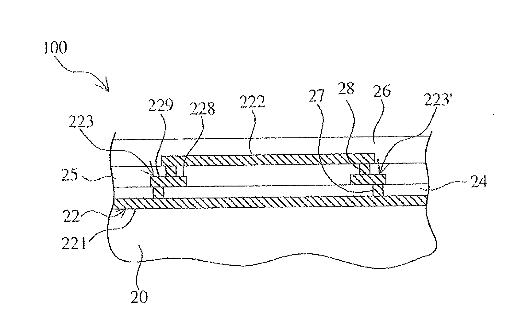
[0031]Referring to FIGS. 4 and 5, an LCD panel 100 according to a first preferred embodiment of the present invention is illustrated and comprises an array substrate of thin film transistor (TFT array substrate) 20, a color filter substrate (CF substrate, not shown), and a layer of liquid crystal material (not shown) between the thin film transistor a...


PUM

PropertyMeasurementUnit
transparent conductiveaaaaaaaaaa
transparentaaaaaaaaaa
lengthaaaaaaaaaa

Abstract

The present invention provides a liquid crystal panel which has a plurality of data lines, a plurality of scan lines and a plurality of display units. Each of the scan lines has a second metal wiring layer, a third metal wiring layer located above the second metal wiring layer, and two transparent conductive lines. The transparent conductive lines are spaced apart from each other and located between the second and third metal wiring layers. The second and third metal wiring layers can form a parallel connection by electrically connecting the second metal wiring layer with the third metal wiring layer, so that the impedance of the scan lines can be reduced.

Description

FIELD OF THE INVENTION[0001]The present invention relates to a liquid crystal panel, and more particularly to a liquid crystal panel for improving the quality of the display of the panel.BACKGROUND OF THE INVENTION[0002]Recently, with the development of semiconductor technology and manufacturing art, thin film transistor liquid crystal display (TFT-LCD) has the features of higher quality, lower power consumption, less radiation, and smaller size so it is gradually becoming a mainstream product in the market. An LCD panel generally comprises an array substrate of thin film transistors, a color filter substrate, and a layer of liquid crystal material between the thin film transistor array substrate and the color filter substrate. A plurality of scan lines are vertically interlaced with a plurality of data lines on the array substrate which delimits a plurality of pixel areas, and a plurality of pixel driving circuits driving the pixels. Wherein the color filter substrate is a transpar...

Claims


Application Information

Patent Timeline
Patent Type & Authority Applications(United States)
IPC IPC(8): G02F1/1362G02F1/1333G02F1/1335G02F1/1368
CPCG02F1/136286G02F1/133514G02F1/133345G02F1/1368G02F1/13629G02F1/136295
Inventor HAN, BINGWANG, JIN JIE
Owner SHENZHEN CHINA STAR OPTOELECTRONICS TECH CO LTD
Why Eureka
Try Eureka