

Plating method and plating apparatus
- Summary
- Abstract
- Description
- Claims
- Application Information
AI Technical Summary
Benefits of technology
Problems solved by technology
Method used
Image

Examples
Embodiment Construction
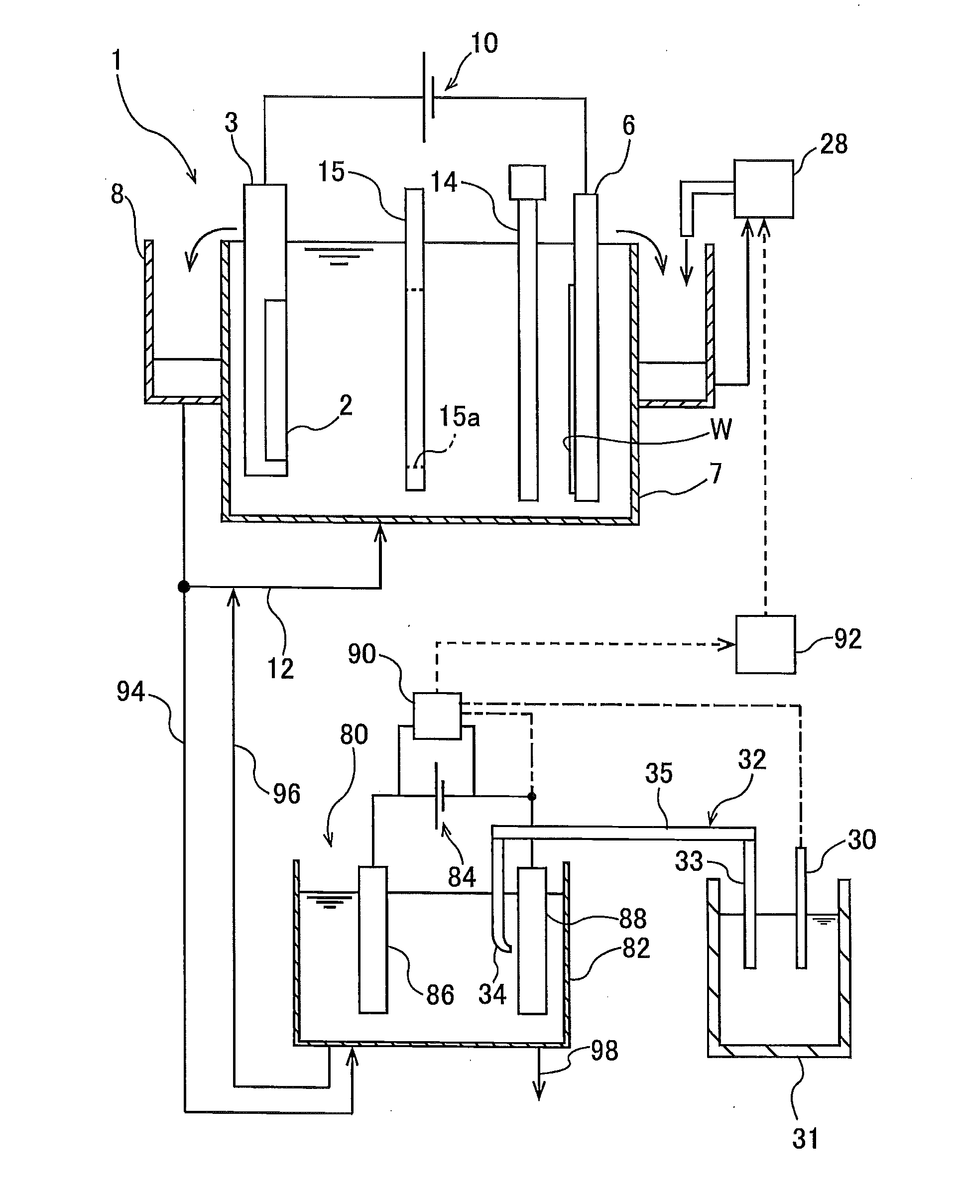
[0046]Embodiments will be described below with reference to the drawings. In FIGS. 1 through 18, identical or corresponding components will be denoted by identical reference numerals, and repetitive descriptions thereof are omitted. The following embodiments show examples of filling a via-hole, formed in a surface of a substrate, with copper.
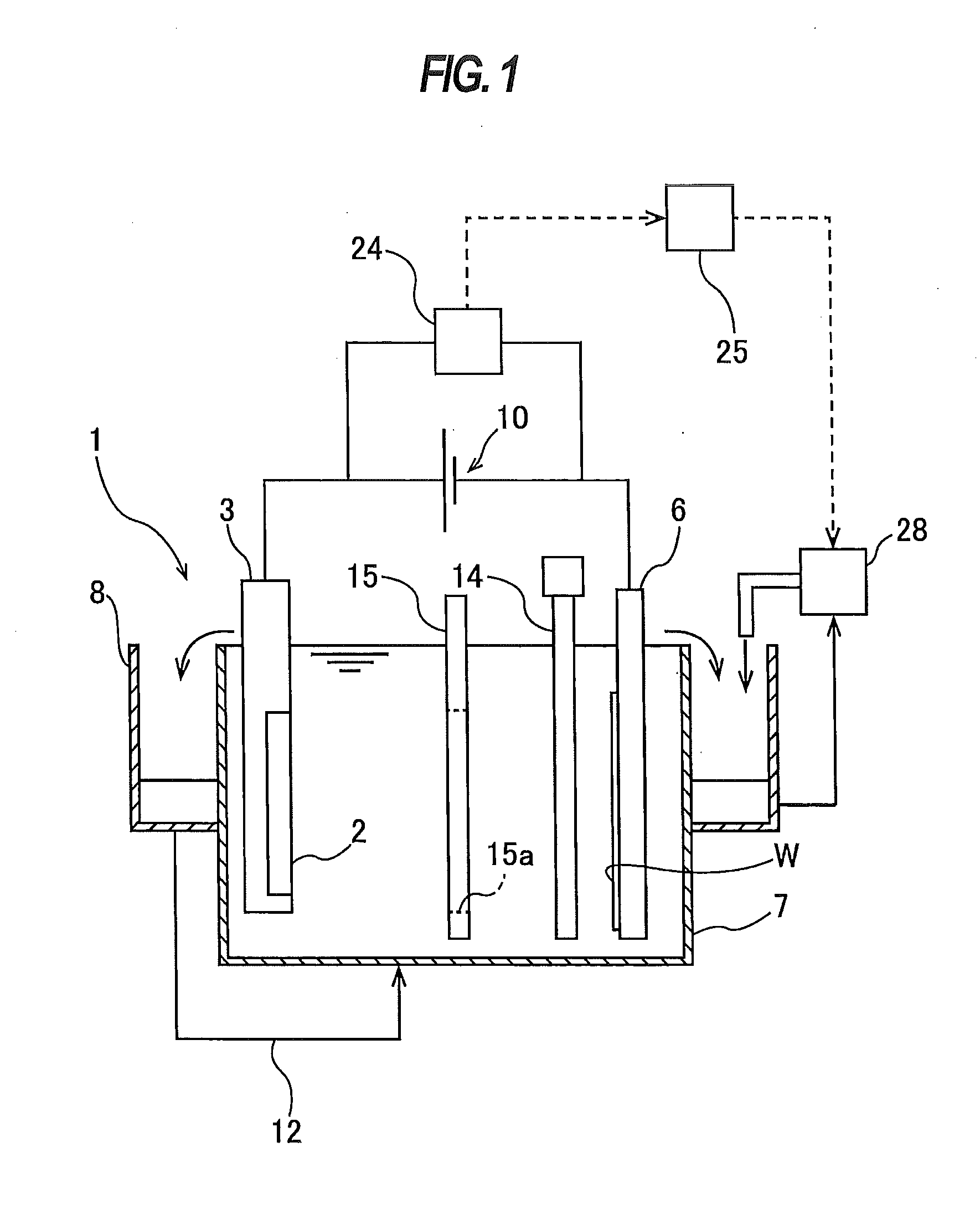
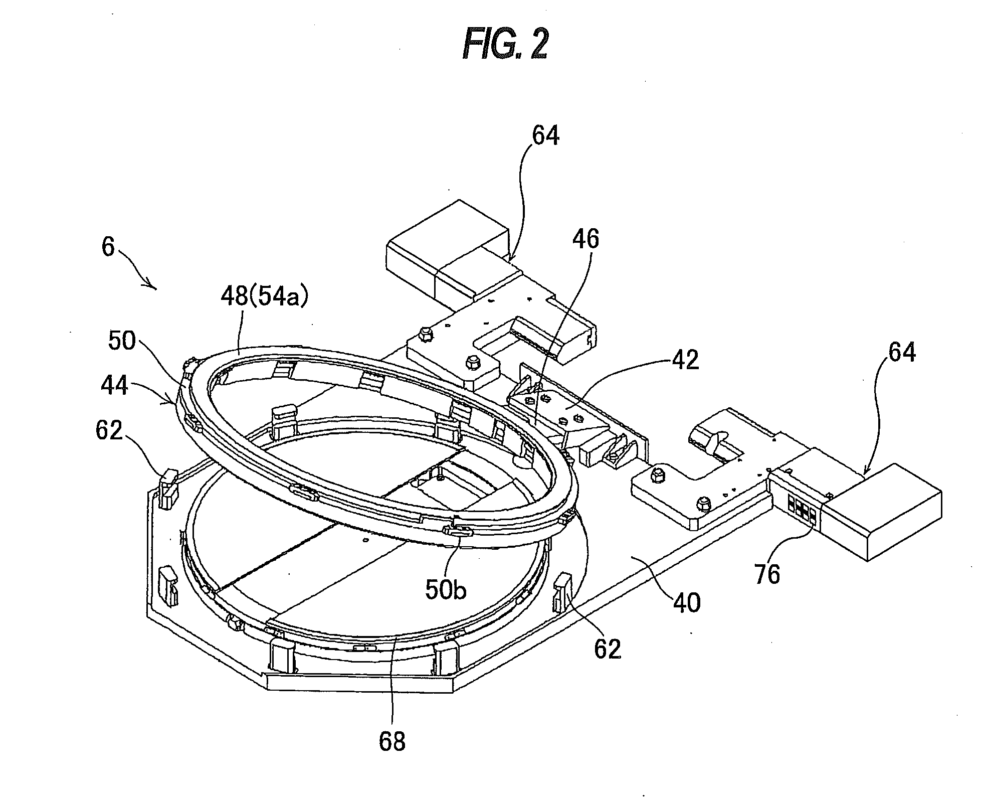
[0047]FIG. 1 is a schematic view showing an embodiment of a plating apparatus. As shown in FIG. 1, the plating apparatus includes a plating bath 1, which has an inner bath 7 for storing a plating solution therein and an overflow bath 8 adjacent to the inner bath 7. The plating solution overflows an upper edge of the inner bath 7 into the overflow bath 8. One end of a plating-solution circulation line 12 for circulating the plating solution is connected to a bottom of the overflow bath 8, and other end of the plating-solution circulation line 12 is connected to a bottom of the inner bath 7. The plating solution that has flowed into the overflow b...
PUM
| Property | Measurement | Unit |
|---|---|---|
| Time | aaaaa | aaaaa |
| Concentration | aaaaa | aaaaa |
| Electric potential / voltage | aaaaa | aaaaa |
Abstract
Description
Claims
Application Information