

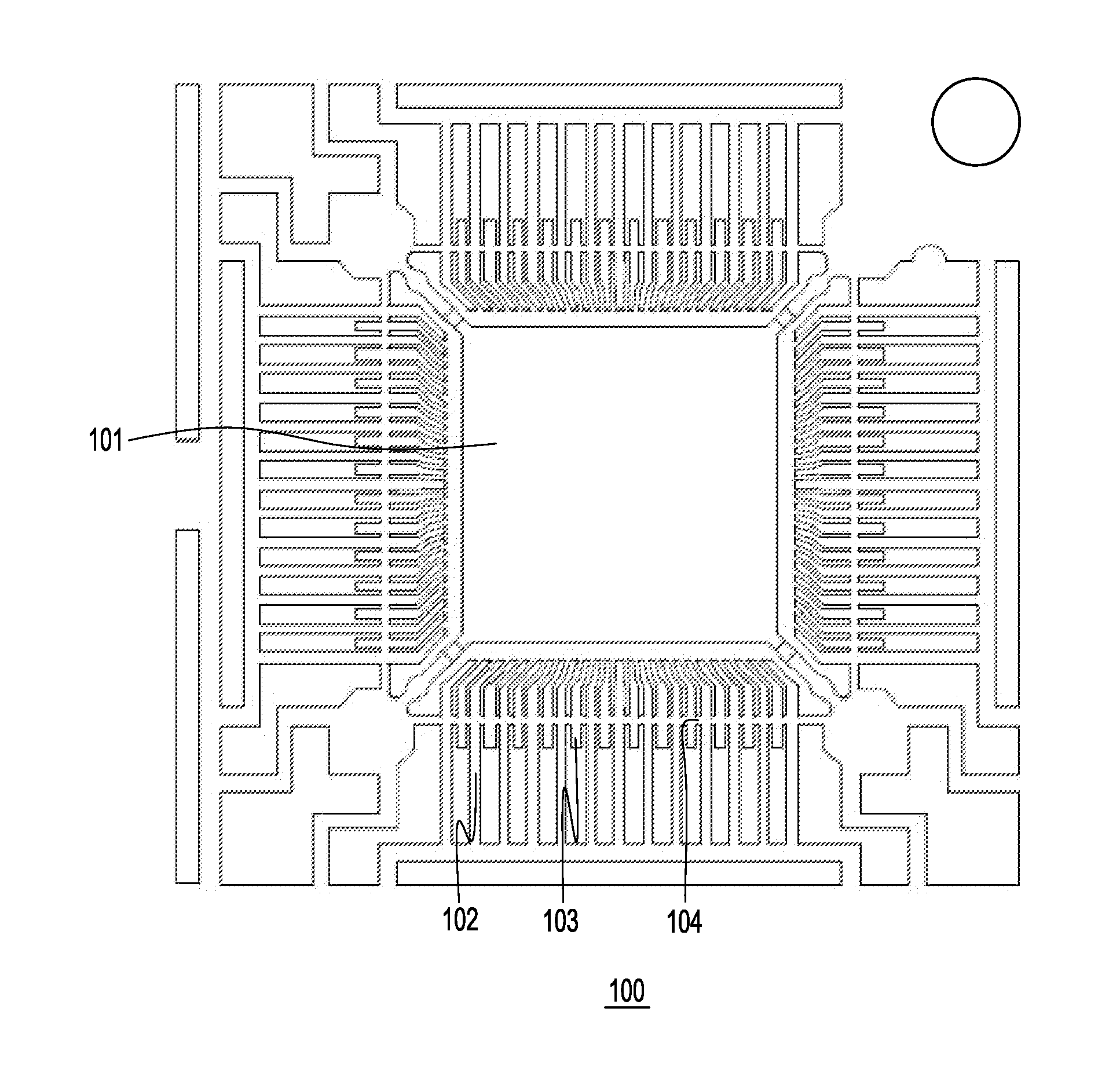
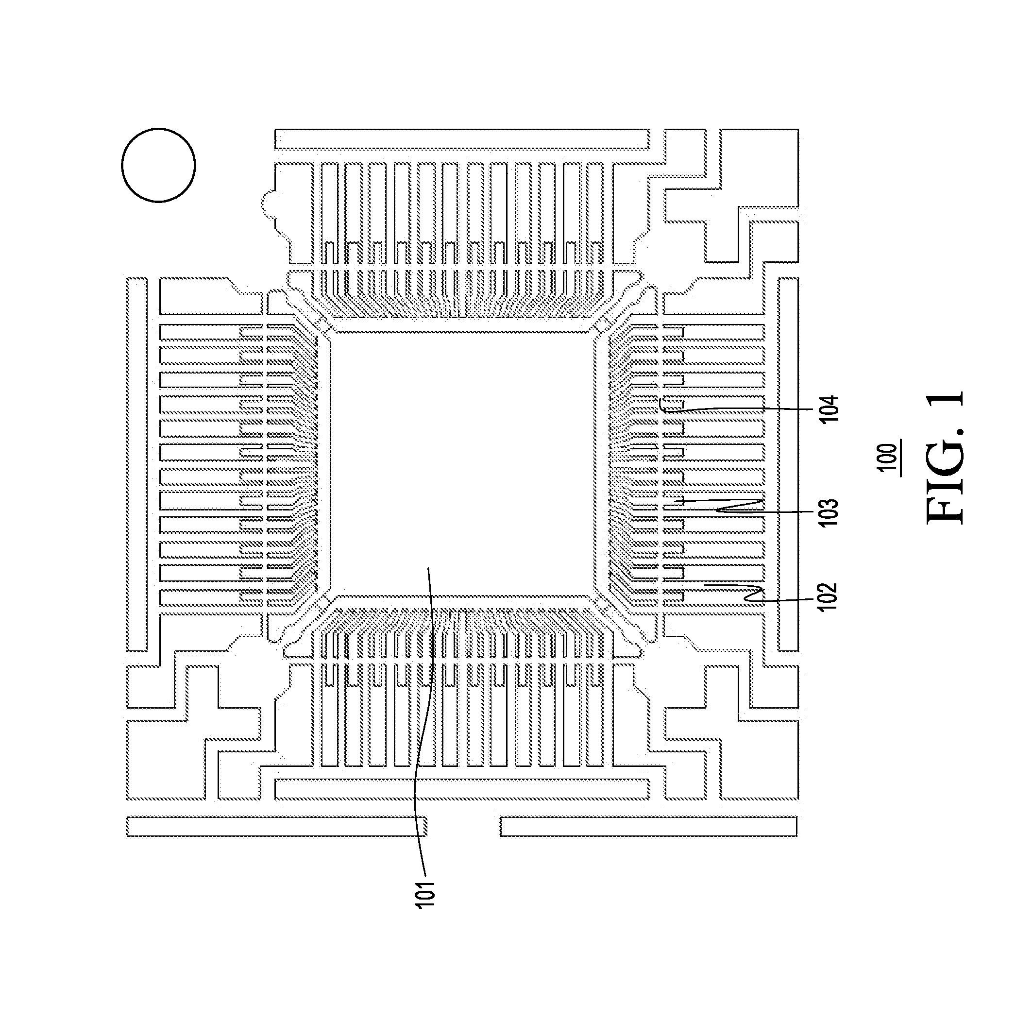
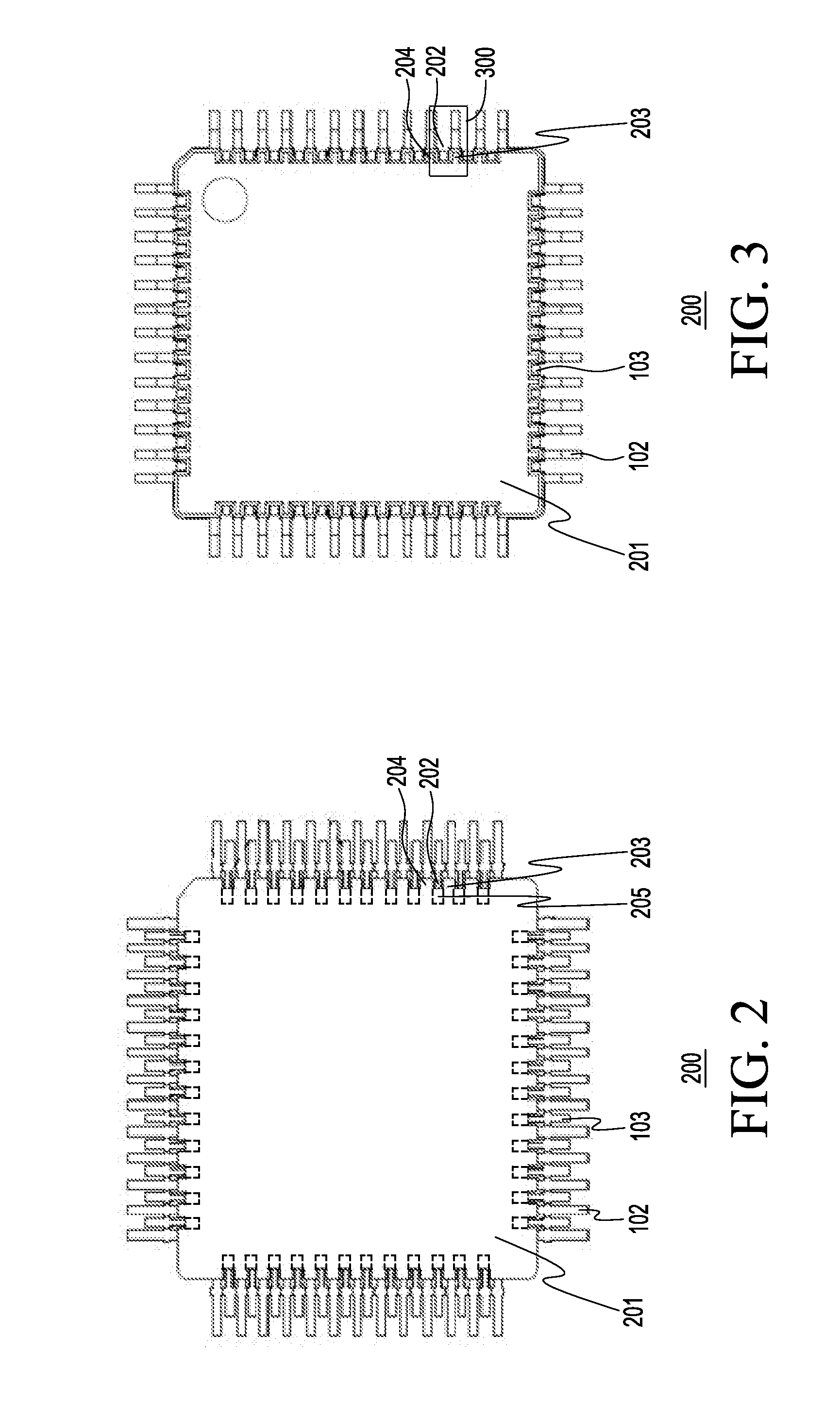
Semiconductor device with webbing between leads
a technology of webbing and semiconductors, applied in semiconductor devices, semiconductor/solid-state device details, electrical apparatus, etc., can solve problems such as the risk of electrical shorts between adjacent leads and electrical shorts
- Summary
- Abstract
- Description
- Claims
- Application Information
AI Technical Summary
Benefits of technology
Problems solved by technology
Method used
Image

Examples
Embodiment Construction
[0014]Detailed illustrative embodiments of the present invention are disclosed herein. However, specific structural and functional details disclosed herein are merely representative for purposes of describing example embodiments of the present invention. Embodiments of the present invention may be embodied in many alternative forms and should not be construed as limited to only the embodiments set forth herein. Further, the terminology used herein is for the purpose of describing particular embodiments only and is not intended to be limiting of example embodiments of the invention.
[0015]As used herein, the singular forms “a,”“an,” and “the,” are intended to include the plural forms as well, unless the context clearly indicates otherwise. It further will be understood that the terms “comprises,”“comprising,”“has,”“having,”“includes,” and / or “including” specify the presence of stated features, steps, or components, but do not preclude the presence or addition of one or more other feat...
PUM
 Abstract
Description
Claims
Application Information