Display panel and display device

a display panel and display panel technology, applied in the direction of basic electric elements, semiconductor devices, electrical equipment, etc., can solve the problems of increased step of the transfer concave shape, serious display defect due to staining,

Active Publication Date: 2015-07-23
SAMSUNG DISPLAY CO LTD
View PDF5 Cites 47 Cited by
  • Summary
  • Abstract
  • Description
  • Claims
  • Application Information

AI Technical Summary

Benefits of technology

[0020]The pixel defining layer may include one of photoresist, polyacrylate-based resin, polyimide-based resin, acryl-based resin, silicon dioxide and silicon nitride, the first edge side surface forming an angle with a surface of the substrate that is larger than about 10 degrees and is less than 90 degrees. The second electrode may be arranged within ...

Problems solved by technology

Particularly, when the thickness of the layer arranged on the via hole is thick, the step of th...

Method used


Image

  • Display panel and display device
  • Display panel and display device
  • Display panel and display device

Examples


Embodiment Construction

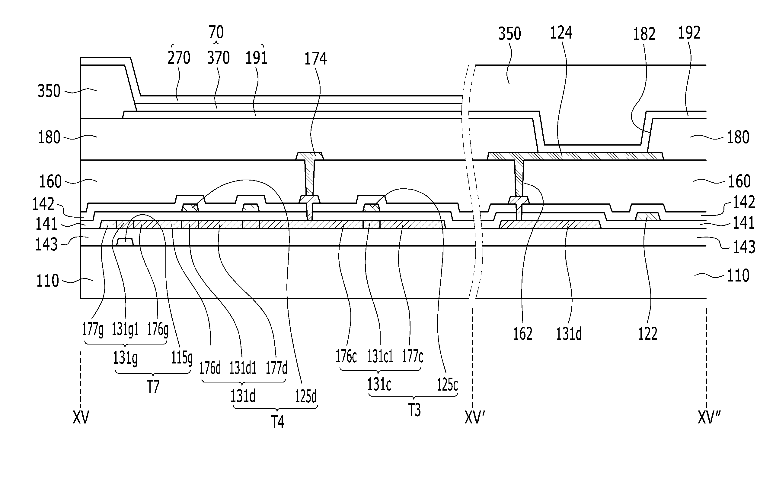
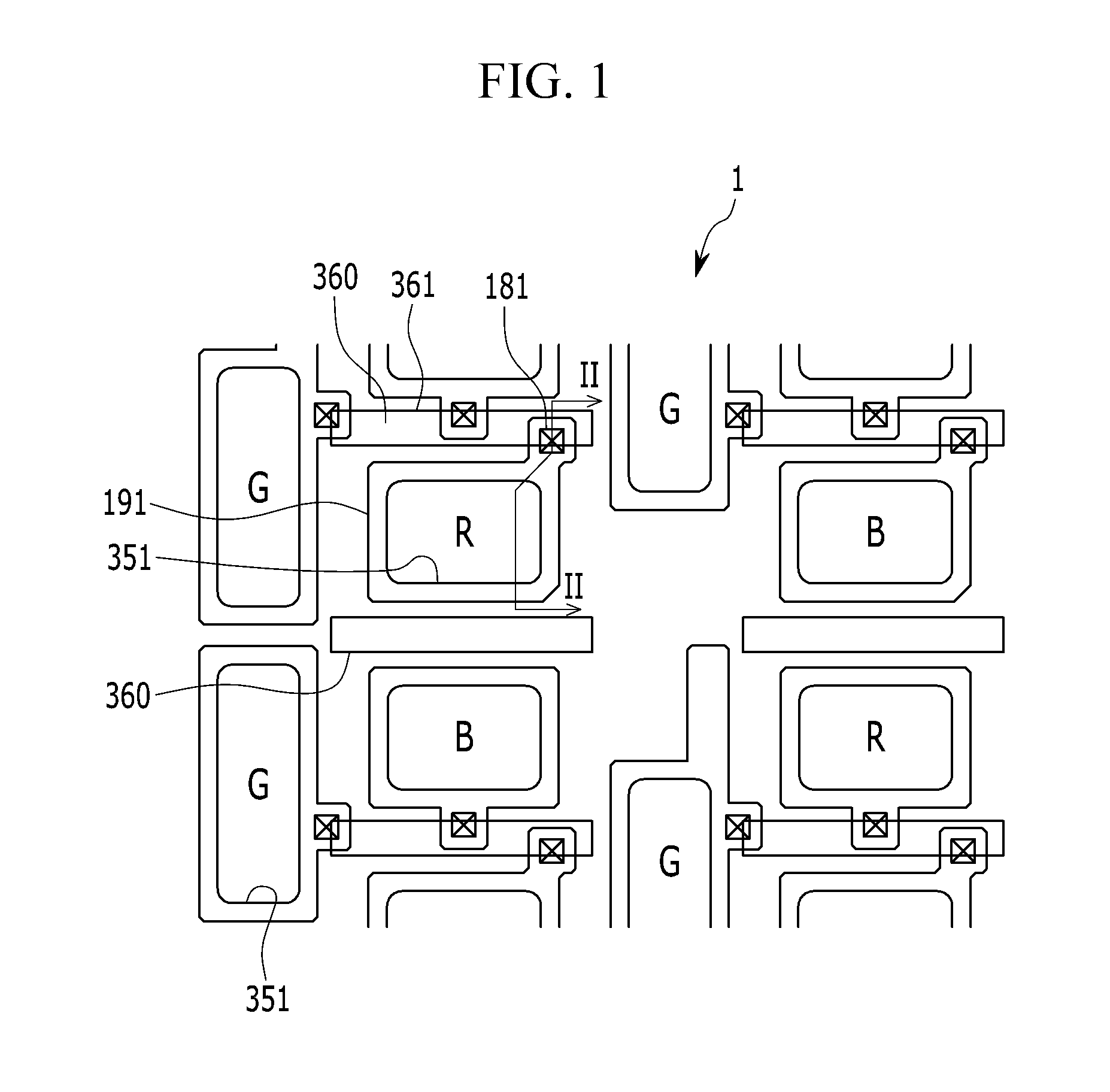
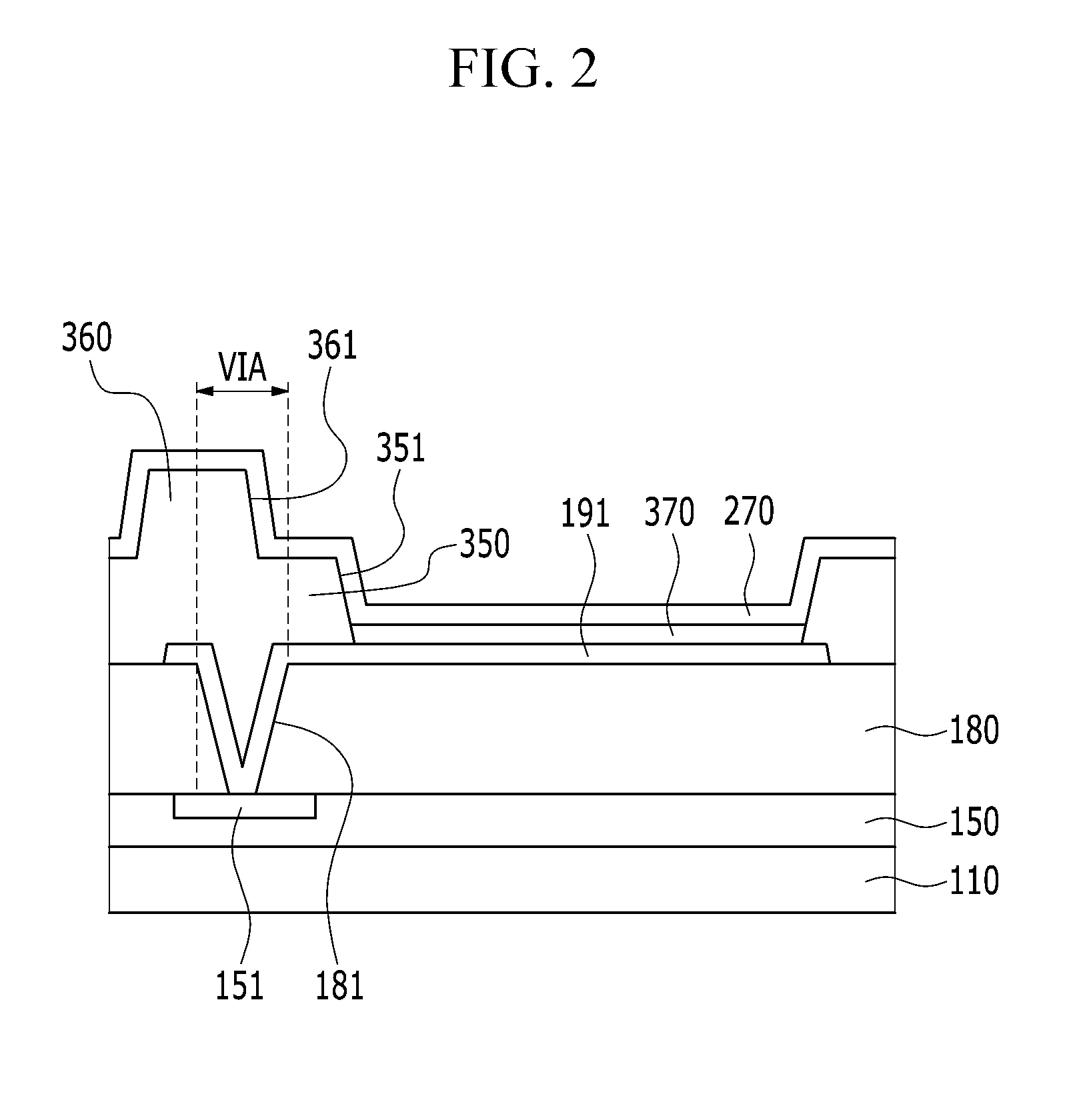
[0033]The present invention will be described more fully hereinafter with reference to the accompanying drawings, in which exemplary embodiments of the invention are shown. As those skilled in the art would realize, the described embodiments may be modified in various different ways, all without departing from the spirit or scope of the present invention.

[0034]In order to clarify the present invention, parts that are not connected with the description will be omitted, and the same elements or equivalents are referred to by the same reference numerals throughout the specification.

[0035]In the drawings, the thickness of layers, films, panels, regions, etc., are exaggerated for clarity. Like reference numerals designate like elements throughout the specification. It will be understood that when an element such as a layer, film, region, or substrate is referred to as being “on” another element, it can be directly on the other element or intervening elements may also be present. In contr...


PUM


Abstract

A display panel and a display device, such as an organic light emitting panel that includes a spacer. The display panel and the display device include a semiconductor element including a first electrode; a passivation layer arranged on the semiconductor element and including a via hole exposing the first electrode; a second electrode arranged on the passivation layer and connected to the first electrode through the via hole; and a spacer arranged on the second electrode and adjacent to the via hole, wherein the spacer exposes at least a portion of a region where the via hole is formed.

Description

CLAIM OR PRIORITY[0001]This application claims priority to and the benefit of Korean Patent Application No. 10-2014-0008272 filed in the Korean Intellectual Property Office on Jan. 23, 2014, the entire contents of which are incorporated herein by reference.BACKGROUND OF THE INVENTION[0002]1. Field of the Invention[0003]The present invention relates to a display panel and a display device. More particularly, the present invention relates to an organic light emitting panel including a spacer and a display device including the same.[0004]2. Description of the Related Art[0005]A display device such as a liquid crystal display (LCD), an organic light emitting diode (OLED) display, and an electrophoretic display includes a field generating electrode and an electro-optical active layer. For example, the organic light emitting diode (OLED) display device includes an organic light emitting layer as the electro-optical active layer. The field generating electrode is connected to a switching e...

Claims


Application Information

Patent Timeline
IPC IPC(8): H01L51/52H01L27/32
CPCH01L27/3276H01L51/5203H10K59/122H10K50/8428H10K50/805H10K59/131
Inventor HWANG, WON MI
Owner SAMSUNG DISPLAY CO LTD
Why Eureka
Try Eureka