

Conductor and method of manufacturing the same
- Summary
- Abstract
- Description
- Claims
- Application Information
AI Technical Summary
Benefits of technology
Problems solved by technology
Method used
Image

Examples
examples
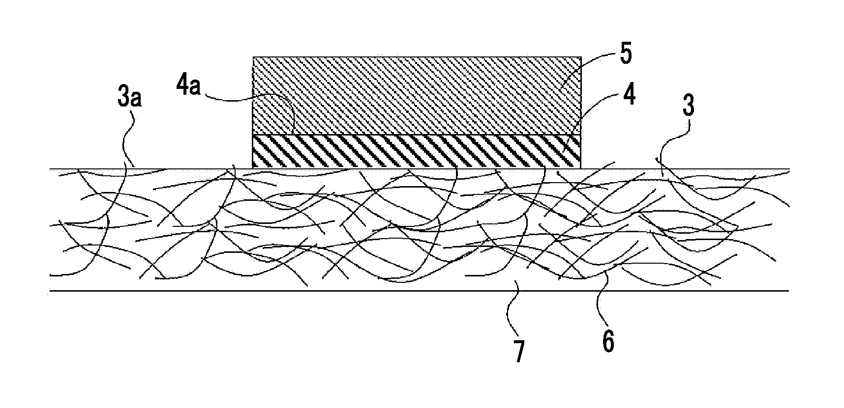
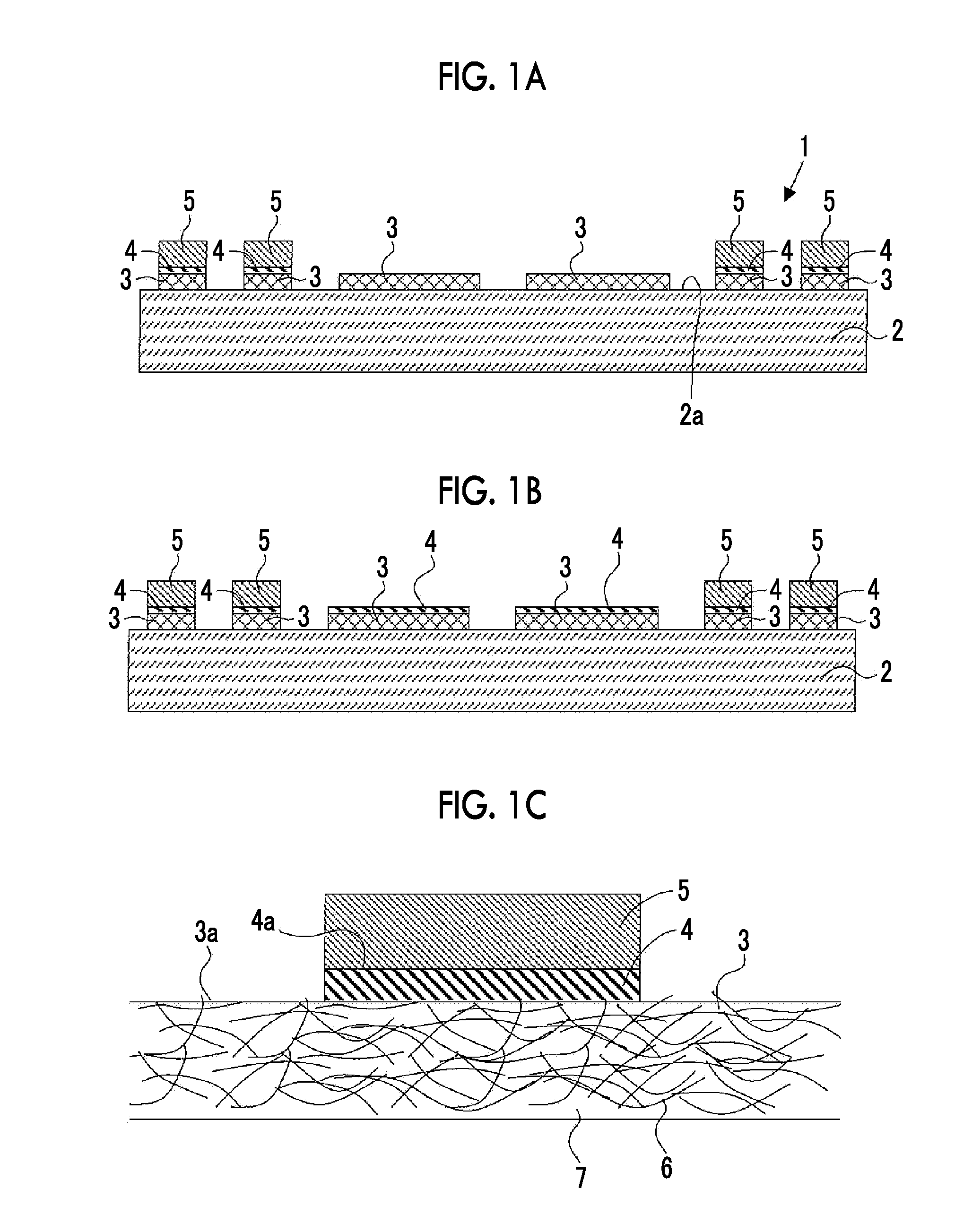
[0063]In an experiment, conductors of Comparative Examples 1 to 4 and Examples 1 to 8 were formed.
[0064]In all of the conductors, a common conductive substrate in which a transparent conductive film including silver nanowires is formed on a transparent substrate was used, and a Cu film having a film thickness of 150 nm was further formed as a metal film.
TABLE 1Cross-cut testresultsPre-treatment conditionsEdgeCenterComparativeAbsentCCExample 1ComparativeUV-ozoneCCExample 2ComparativeExcimer UVCCExample 3ComparativeOnly reverse sputteringCCExample 4Example 1ITO buffer film (20 nm)BBExample 2ITO buffer film (100 nm)BBExample 3Reverse sputtering & ITO buffer filmAA(2 nm)Example 4Reverse sputtering & ITO buffer filmAA(20 nm)Example 5Reverse sputtering & ITO buffer filmAA(100 nm)Example 6Reverse sputtering & ITO buffer filmAA(20 mm)=>leaving in atmosphere reverse sputteringExample 7TES treatmentAAExample 8P-TES treatmentAA
[0065]As shown in Table 1, in Comparative Example 1, before forming...
PUM
| Property | Measurement | Unit |
|---|---|---|
| Structure | aaaaa | aaaaa |
| Adhesion strength | aaaaa | aaaaa |
| Electrical conductor | aaaaa | aaaaa |
Abstract
Description
Claims
Application Information