

Thin film capacitor, circuit board incorporating the same, and thin film capacitor manufacturing method
- Summary
- Abstract
- Description
- Claims
- Application Information
AI Technical Summary
Benefits of technology
Problems solved by technology
Method used
Image

Examples
examples
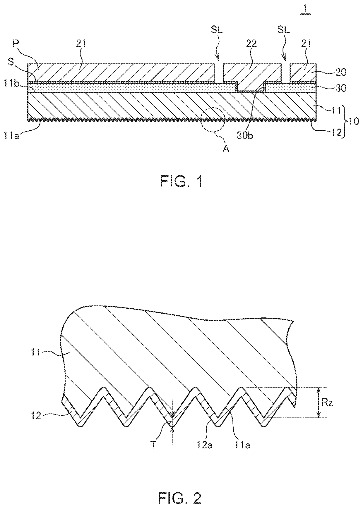
[0045]There were fabricated samples having the same layer structure as that illustrated in FIG. 1 except that the through hole 30b and slit SL were omitted. Then, as illustrated in FIG. 9, each sample was attached to the insulating resin layer 41, followed by peeling (peel test). In these samples, Ni having a 10 μm thickness was used for the first metal layer 11 constituting the lower electrode layer 10, Ni having a 0.5 μm thickness and Cu having a 10 μm thickness were for the upper electrode layer 20, and barium titanate having a 0.6 μm thickness was for the dielectric layer 30. For the second metal layer 12, Cu films having different thicknesses were used for respective samples. The surface roughness Rz of the surface 11a of the first metal layer 11 was set to 1 μm, 2 μm, or 5 μm. The insulating base 40 was constituted using a glass epoxy substrate (thickness: 600 μm), and the insulating resin layer 41 was formed of epoxy resin (thickness: 25 μm) including filler.
[0046]Then, the i...
PUM
 Abstract
Description
Claims
Application Information