

Thin film capacitor, manufacturing method therefor, and multilayer circuit board embedded with thin film capacitor
- Summary
- Abstract
- Description
- Claims
- Application Information
AI Technical Summary
Benefits of technology
Problems solved by technology
Method used
Image

Examples
first embodiment
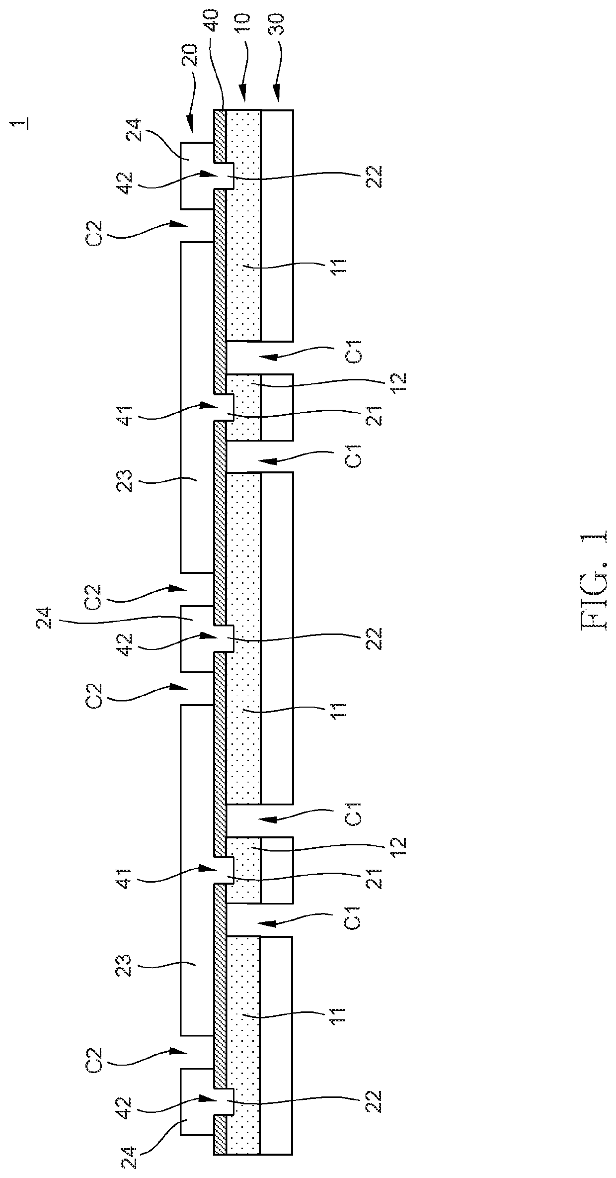
[0029]FIG. 1 is a schematic cross-sectional view for explaining the structure of a thin film capacitor 1 according to the present invention.
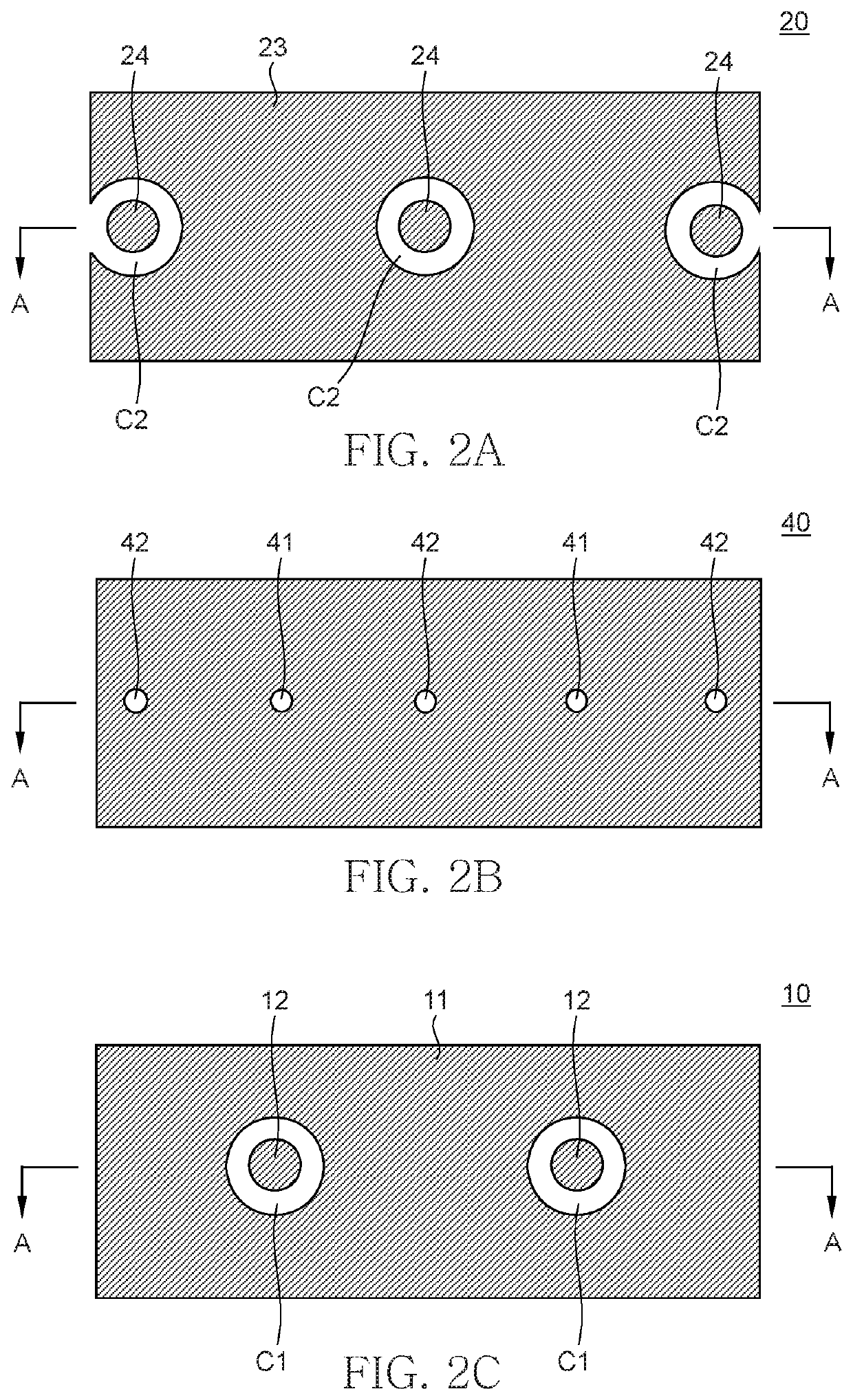
[0030]As illustrated in FIG. 1, the thin film capacitor 1 according to the first embodiment includes a capacitive insulating film 40, first and second metal films 10 and 20 formed on the front and back sides of the capacitive insulating film 40, respectively, and a third metal film 30 provided so as to overlap the first metal film 10. FIGS. 2A to 2C are schematic plan views of respective layers constituting the thin film capacitor 1. FIG. 2A illustrates the shape of the second metal film 20, FIG. 2B illustrates the shape of the capacitive insulating film 40, and FIG. 2C illustrates the shape of the first metal film 10. FIG. 1 illustrates a cross section taken along line A-A in FIGS. 2A to 2C.
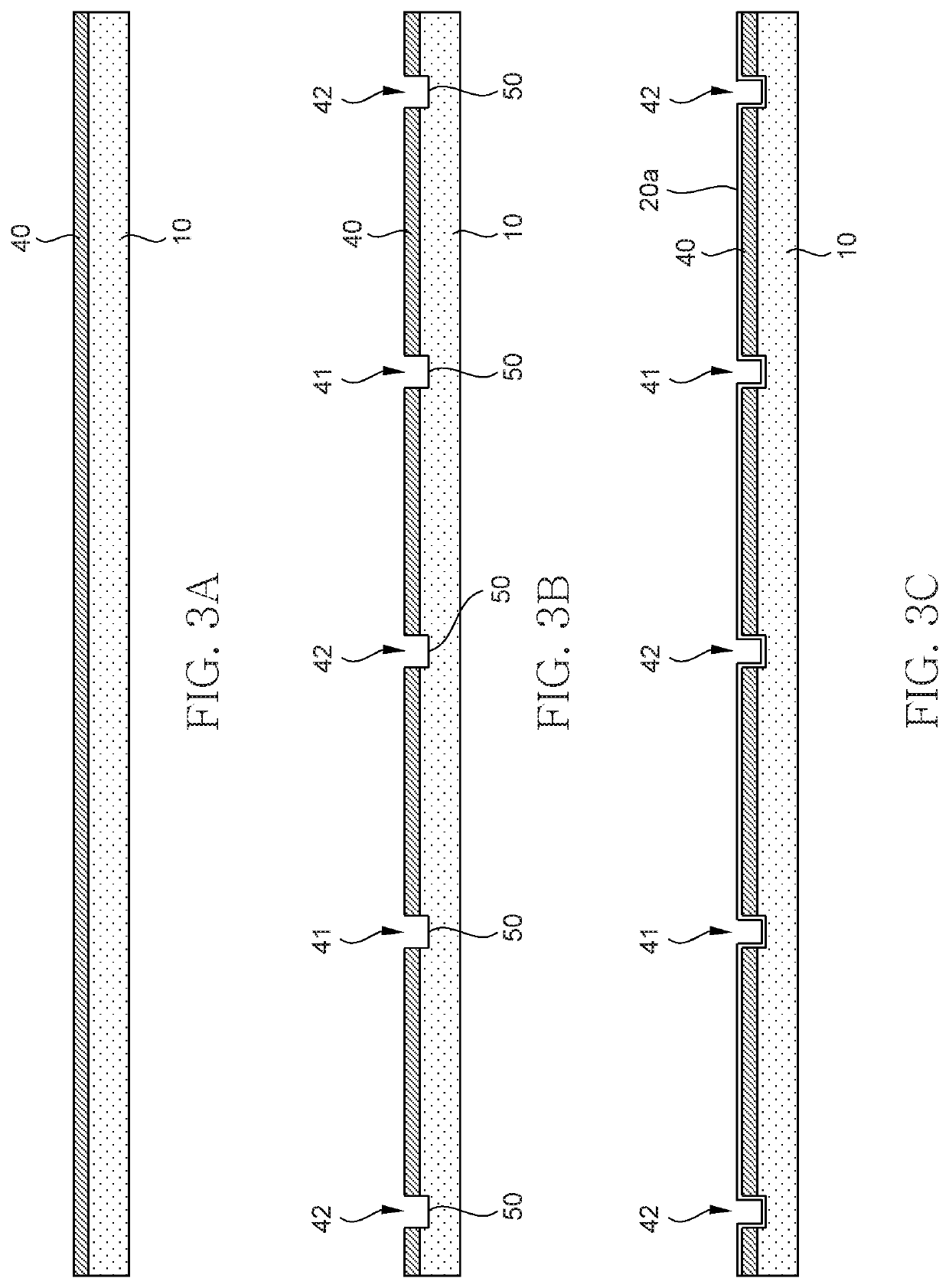
[0031]The capacitive insulating film 40 is made of a ceramic material having a perovskite structure, such as barium titanate. First through holes 41 and sec...
second embodiment
[0051]FIG. 8 is a schematic cross-sectional view for explaining the structure of a thin film capacitor 2 according to the present invention.
[0052]As illustrated in FIG. 8, the thin film capacitor 2 according to the second embodiment differs from the thin film capacitor 1 according to the first embodiment in that a barrier metal 70 is provided as the base of the second metal film 20. Other configurations are the same as those of the thin film capacitor 1 according to the first embodiment, so the same reference numerals are given to the same elements, and overlapping description will be omitted.
[0053]The barrier metal 70 is provided for preventing migration from the second metal film 20 to the first metal film 10. As the material of the barrier metal 70, a material having a higher melting point than the second metal film 20, such as tungsten, can be used.
third embodiment
[0054]FIG. 9 is a schematic cross-sectional view for explaining the structure of a thin film capacitor 3 according to the present invention.
[0055]As illustrated in FIG. 9, the thin film capacitor 3 according to the third embodiment differs from the thin film capacitor 1 according to the first embodiment in that the third metal film 30 is omitted. Other configurations are the same as those of the thin film capacitor 1 according to the first embodiment, so the same reference numerals are given to the same elements, and overlapping description will be omitted.
[0056]As exemplified in the present embodiment, the third metal film 30 may not necessarily be provided in the present invention, and the first metal film 10 made of Ni or the like may be used directly as an external terminal.
[0057]FIG. 10 is a schematic cross-sectional view for explaining the structure of a multilayer circuit board 80 embedded with the thin film capacitor 1 according to the first embodiment.
[0058]In the example i...
PUM
 Abstract
Description
Claims
Application Information