Semiconductor device comprising an ESD protection device, an ESD protection circuitry, an integrated circuit and a method of manufacturing a semiconductor device

a technology of esd protection device and semiconductor device, which is applied in the direction of semiconductor devices, electrical devices, transistors, etc., can solve the problems of large voltage, affecting the manufacturing efficiency of semiconductor devices, and affecting the performance of semiconductor devices

Active Publication Date: 2015-08-06
NXP USA INC
View PDF9 Cites 1 Cited by
  • Summary
  • Abstract
  • Description
  • Claims
  • Application Information

AI Technical Summary

Problems solved by technology

Electrostatic discharge (ESD) is a problem in the utilization, manufacturing and / or design of the semiconductor devices.
The integrated circuits manufactured on the semiconductor device can be damaged when ESD events are received from other circuits coupled to the semiconductor device or from people and / or machinery and tools touching the semiconductor device.
During an ESD event, the integrated circuit may receive a charge which leads to relatively large voltages during a relatively short period of time.
These currents may cause irreparable damage to the integrated circuit.
In many applications, a strong snapback behaviour is not desired and, in other application, even no snapback behaviour is allowed.
Consequently, the ESD protection device of the cited patent application can not be used in such applications.

Method used


Image

  • Semiconductor device comprising an ESD protection device, an ESD protection circuitry, an integrated circuit and a method of manufacturing a semiconductor device
  • Semiconductor device comprising an ESD protection device, an ESD protection circuitry, an integrated circuit and a method of manufacturing a semiconductor device
  • Semiconductor device comprising an ESD protection device, an ESD protection circuitry, an integrated circuit and a method of manufacturing a semiconductor device

Examples


Embodiment Construction

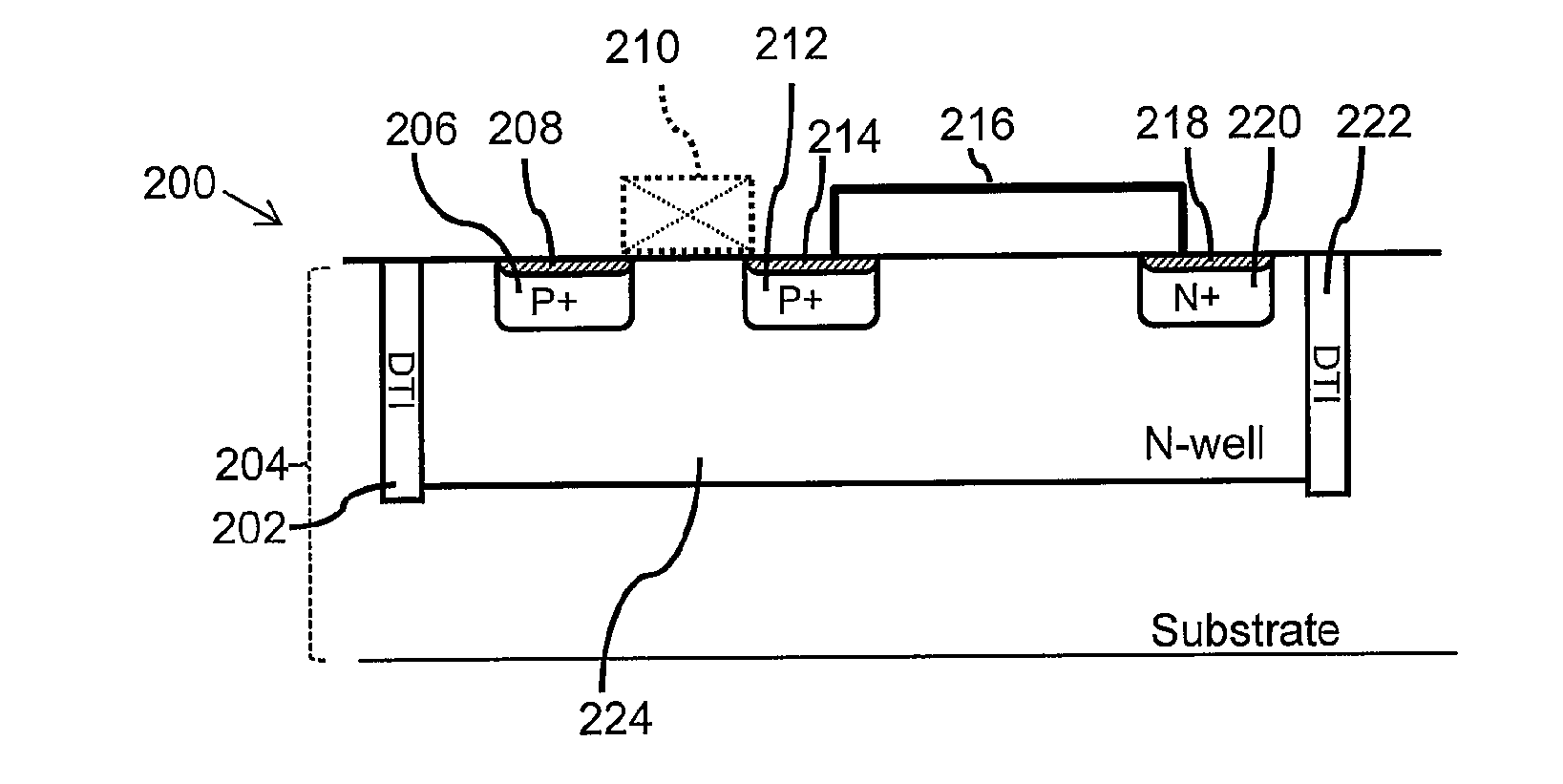
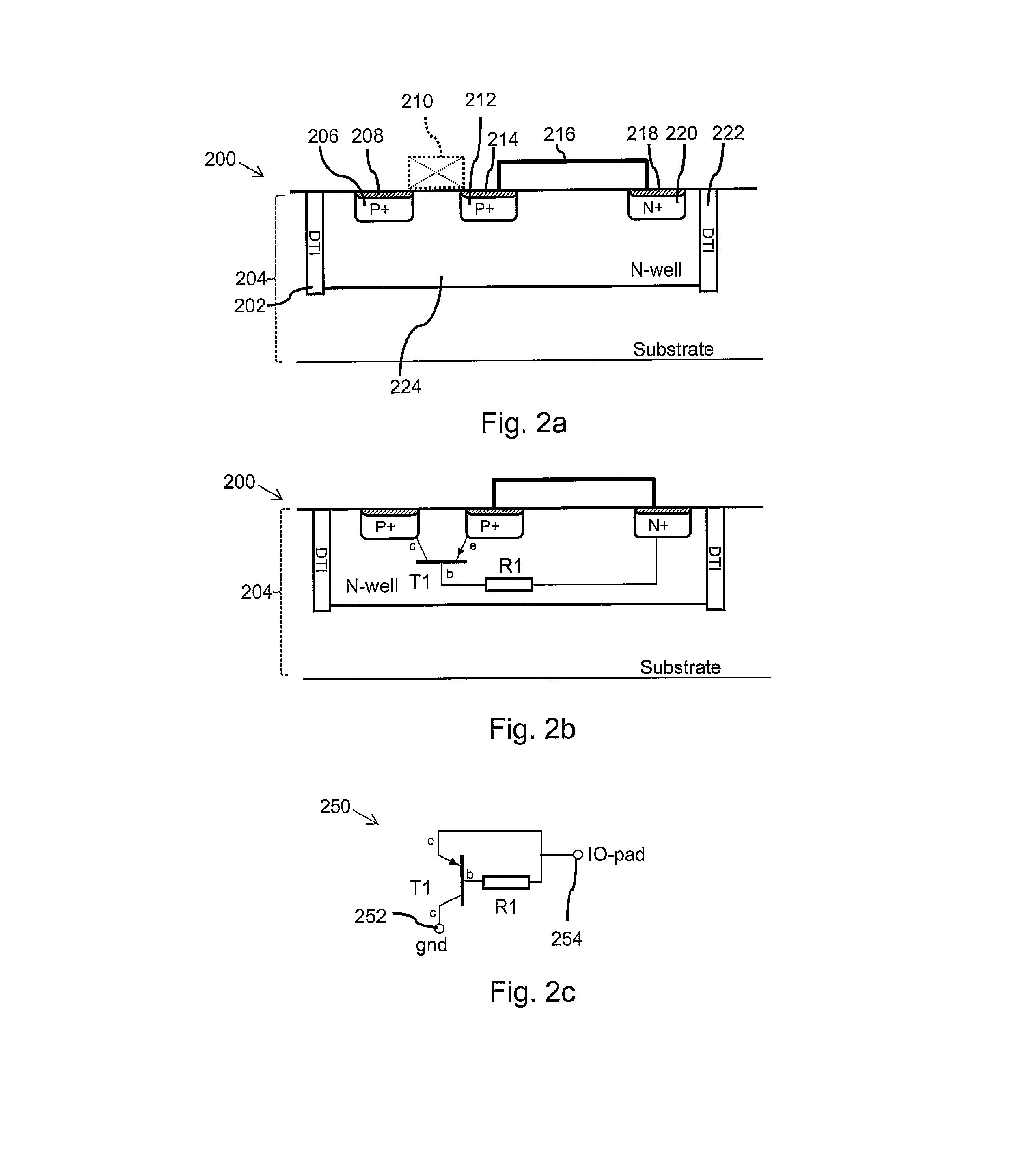
[0018]FIG. 2a schematically presents a cross-sectional view of an example of a structure of the ESD protection device 200 in a substrate 204. In the example of FIG. 2a the substrate 204 is of a P-type. In this P-type substrate 204, an isolated N-well 224 is created which is isolated from neighbouring structures by Deep Trench Isolation formed by structures 202, 222 (DPI). The N-well 224 is a region in the substrate 204 with a majority of N-dopants. The sheet resistance of the N-well 224 is at least 150 Ohmsq. In another embodiment, the sheet resistance of the N-well 224 is at least 300 Ohmsq. In yet a further embodiment, the sheet resistance of the N-well 224 is at least 1.5 kOhmsq. In an area of the N-well 224 an N+ region 220 is manufactured which has a higher N-dopants concentration than the N-well 224. The top-surface of the N+ region 220 is silicided 218 to allow a good electrical connection between the N+ region 220 and an electrical connection 216 which is manufactured in one...


PUM

PropertyMeasurementUnit
trigger voltageaaaaaaaaaa
voltageaaaaaaaaaa

Abstract

A semiconductor device includes an ESD protection device. In a N-well, two P+ doped regions form a collector and emitter of a parasitic transistor of the ESD protection device. The N-well area between the P+ doped regions, forms a base of the parasitic transistor. At some distance away from the P+ doped regions an N+ doped region is provided. The N-well in between the N+ doped region and base of the transistor forms a parasitic resistor of the ESD protection device. The N+ doped region and the emitter of the transistor are coupled to each other via an electrical connection. The ESD protection device has a limited snapback behaviour and has a well-tunable trigger voltage.

Description

FIELD OF THE INVENTION[0001]This invention relates to.BACKGROUND OF THE INVENTION[0002]Electrostatic discharge (ESD) is a problem in the utilization, manufacturing and / or design of the semiconductor devices. The integrated circuits manufactured on the semiconductor device can be damaged when ESD events are received from other circuits coupled to the semiconductor device or from people and / or machinery and tools touching the semiconductor device. During an ESD event, the integrated circuit may receive a charge which leads to relatively large voltages during a relatively short period of time. If, for example, the integrated circuit breaks down as the result of the high voltage and starts to conduct the charge of the ESD event, a current of several amperes may flow through the integrated circuit during a relatively short period of time. These currents may cause irreparable damage to the integrated circuit.[0003]Today most integrated circuit comprise ESD protection circuitries that are ...

Claims


Application Information

Patent Timeline
Patent Type & Authority Applications(United States)
IPC IPC(8): H01L27/02H01L29/66
CPCH01L27/0277H01L29/6625H01L27/0259
Inventor LAINE, JEAN PHILIPPEBESSE, PATRICE
Owner NXP USA INC
Why Eureka
Try Eureka