Method for manufacturing semiconductor device and semiconductor device

a manufacturing method and semiconductor technology, applied in semiconductor devices, diodes, transistors, etc., can solve the problems of avalanche breakdown that can occur more easily in the igbt region and the diode region than in the peripheral region, and achieve the effect of high durability against avalanche breakdown

Inactive Publication Date: 2015-08-13
TOYOTA JIDOSHA KK
View PDF3 Cites 27 Cited by
  • Summary
  • Abstract
  • Description
  • Claims
  • Application Information

AI Technical Summary

Benefits of technology

[0006]In this method for manufacturing, when the crystal defects are formed in the n-type region in the diode region, the crystal defects are formed also in the n-type region in the peripheral region. Moreover, when the crystal defects are formed in the n-type region in the IGBT region, the crystal defects are formed also in the n-type region in the peripheral region. Therefore, in the n-type region in the peripheral region, the crystal defects are formed with a density higher than that in the n-type region in the IGBT region and in the n-type region in the diode region. Thus, in the semiconductor device manufactured by this method, avalanche breakdown can occur more easily in the IGBT region and the diode region than in the peripheral region. Therefore, the semiconductor device manufactured by this method has high durability against avalanche breakdown.

Problems solved by technology

Thus, in the semiconductor device manufactured by this method, avalanche breakdown can occur more easily in the IGBT region and the diode region than in the peripheral region.

Method used


Image

  • Method for manufacturing semiconductor device and semiconductor device
  • Method for manufacturing semiconductor device and semiconductor device
  • Method for manufacturing semiconductor device and semiconductor device

Examples


Embodiment Construction

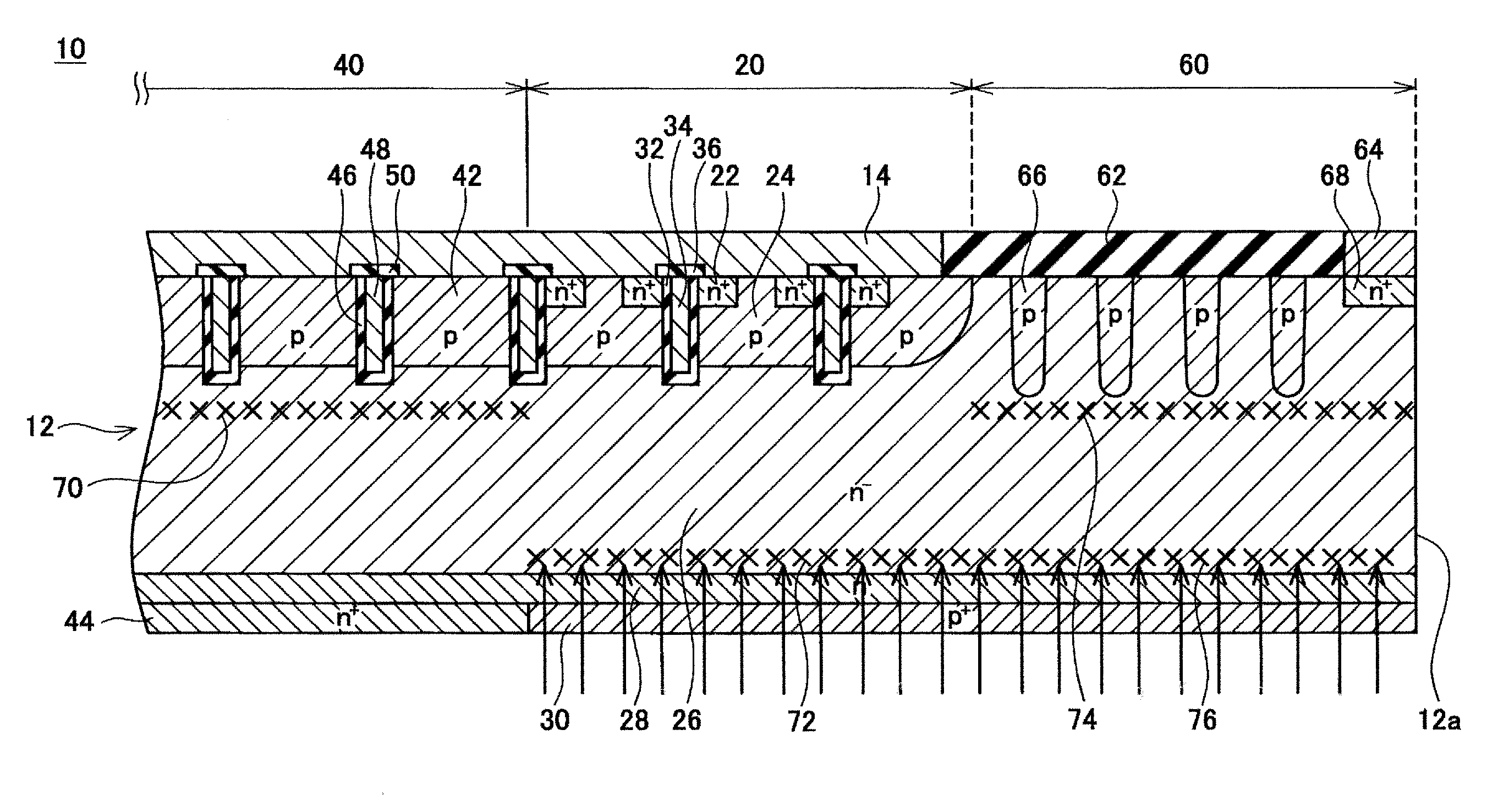
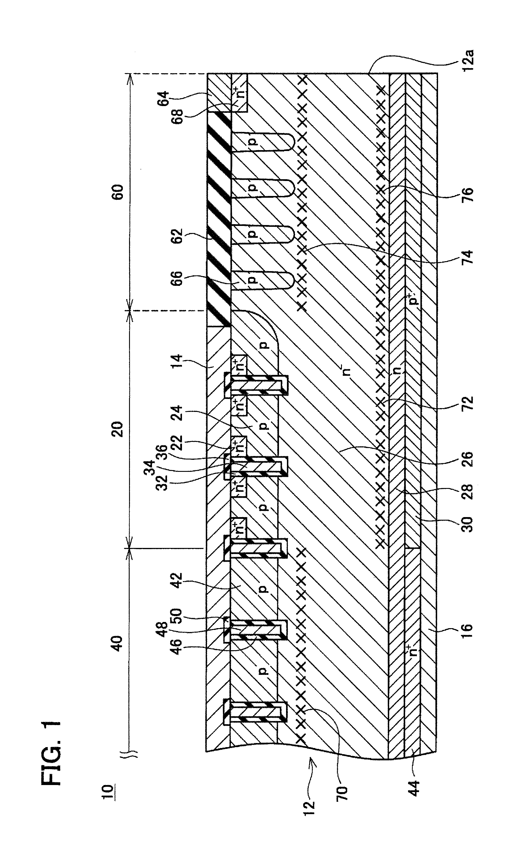
[0013]A semiconductor device 10 of an embodiment illustrated in FIG. 1 comprises a semiconductor substrate 12, a front surface electrode 14 formed on a front surface of the semiconductor substrate 12, and a rear surface electrode 16 formed on a rear surface of the semiconductor substrate 12. The semiconductor substrate 12 is a substrate made of silicon.

[0014]The semiconductor substrate 12 comprises an IGBT region 20 in which a vertical-type IGBT is formed, a diode region 40 in which a vertical-type diode is formed, and a peripheral region 60 on an outer side of the IGBT region 20 and the diode region 40. The peripheral region 60 is formed between the IGBT region 20 and an end face 12a of the semiconductor substrate 12. Alternatively, the peripheral region 60 may be formed between the diode region 40 and the end surface 12a of the semiconductor substrate 12.

[0015]An emitter region 22, a body region 24, a drift region 26, a buffer region 28, and a collector region 30 are formed in the...


PUM


Abstract

A semiconductor device having high durability against avalanche breakdown is provided. A method for manufacturing a semiconductor device is provided with an IGBT region, a diode region, and a peripheral region includes: forming crystal defects in an n-type region by implanting charged particles into an n-type region in the diode region and an n-type region in the peripheral region; and forming crystal defects in the n-type region by implanting charged particles into an n-type region in the IGBT region and the n-type region in the peripheral region.

Description

CROSS-REFERENCE TO RELATED APPLICATION[0001]This application claims priority to Japanese Patent Application No. 2014-023864 filed on Feb. 10, 2014, the contents of which are hereby incorporated by reference into the present application.TECHNICAL FIELD[0002]A technology disclosed in this description relates to a semiconductor device.DESCRIPTION OF RELATED ART[0003]Japanese Patent Application Publication No. 2011-129619 discloses a semiconductor device in which an IGBT and a diode are integrated. Crystal defects formed by implanting charged particles are present in a drift region of the IGBT and a drift region of the diode. Such crystal defects function as recombination centers of carriers. While the diode is on, a part of holes having flowed into the drift region of the diode disappears in the crystal defects. As a result, a rise of concentration of the holes in the drift region of the diode is suppressed, and a recovery characteristic of the diode is improved. While the IGBT is on, ...

Claims


Application Information

Patent Timeline
Patent Type & Authority Applications(United States)
IPC IPC(8): H01L29/06H01L29/739H01L29/66H01L27/06
CPCH01L29/0626H01L27/0635H01L29/66348H01L29/7397H01L29/0696H01L27/0629H01L29/0619H01L29/0638H01L29/32
Inventor HARA, MASAFUMI
Owner TOYOTA JIDOSHA KK
Why Eureka
Try Eureka