Semiconductor device

a technology of semiconductors and semiconductors, applied in the direction of semiconductor devices, electrical devices, transistors, etc., can solve the problems of reduced manufacturing cost and decreased and achieve the effect of increasing the gate width, increasing the current output of transistors, and reducing invalid area on the substra

Active Publication Date: 2015-08-27
ANCORA SEMICON INC
View PDF2 Cites 0 Cited by
  • Summary
  • Abstract
  • Description
  • Claims
  • Application Information

AI Technical Summary

Benefits of technology

[0009]To solve the described problems, the present disclosure provides a semiconductor device having a greater gate width of the gate electrode in the same area of the substrate, and providing greater current.
[0012]In conclusion, the semiconductor device of the present disclosure utilizes the gate electrode with a ring structure to increase the gate width, and thus the current output of the transistors is increased. Furthermore, the shortest distances between every sections of the gate electrode and the first electrode are substantially the same. The shortest distances between every sections of the gate electrode and the second electrode are substantially the same. Therefore, the invalid area on the substrate is decreased, and the manufacturing cost is also decreased.

Problems solved by technology

Therefore, the invalid area on the substrate is decreased, and the manufacturing cost is also decreased.

Method used


Image

  • Semiconductor device
  • Semiconductor device
  • Semiconductor device

Examples


Embodiment Construction

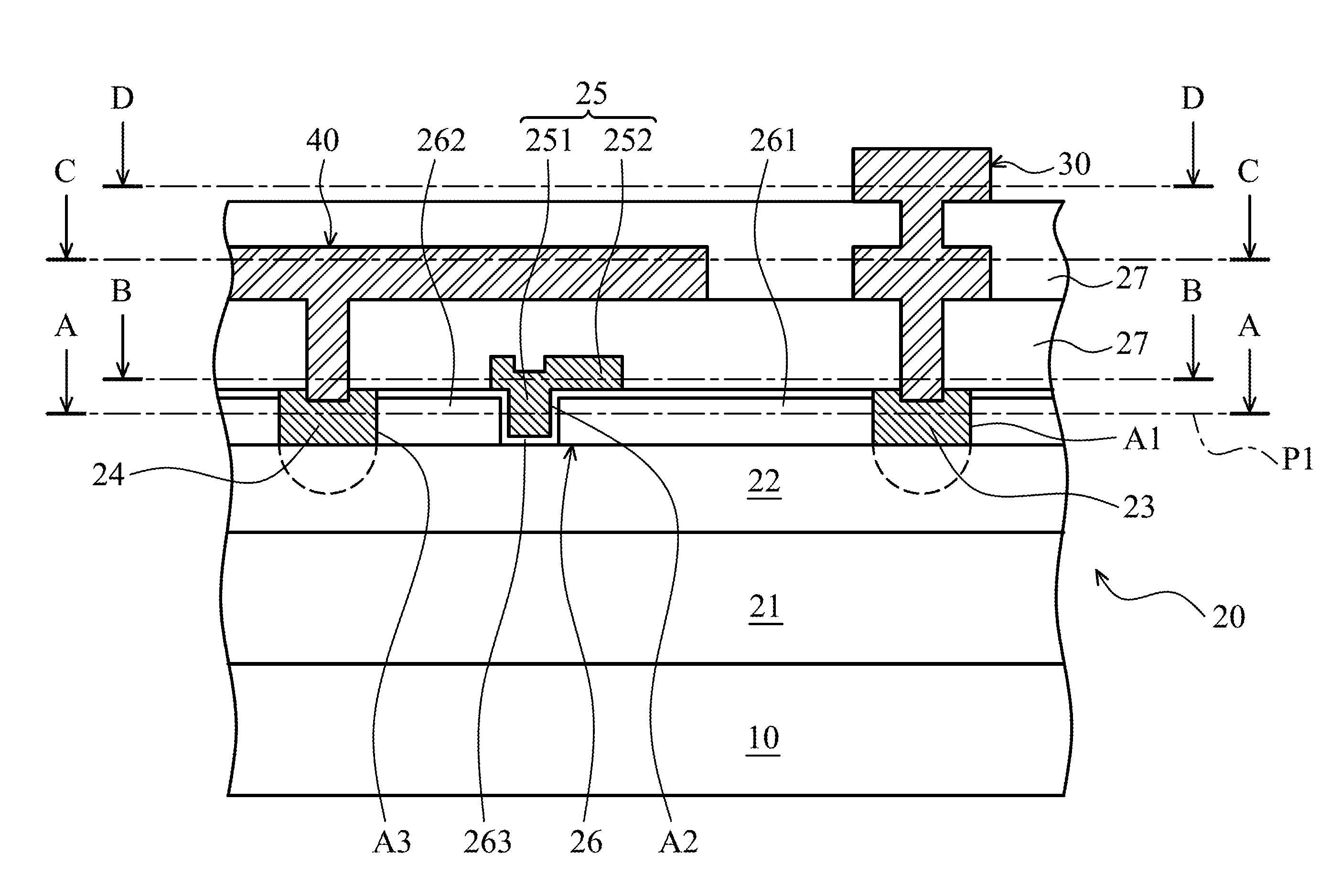
[0022]FIG. 3 is a cross-sectional view of the semiconductor device 1 according to the present disclosure. FIG. 4 is a cross-sectional view along the line AA of FIG. 3. The semiconductor device 1 is a switching device utilized in high power supplies.

[0023]The semiconductor device 1 includes a substrate 10, a plurality of transistors 20, a first conduction layer 30, and a second conduction layer 40. The substrate 10 may be a wafer made of silicon. The transistors 20 may be field-effect transistors (FETs) 20 formed on the substrate 10 and arranged on the substrate 10 in an array.

[0024]In some embodiments, the transistor 20 is a normally-on transistor including a buffer layer 21, an active layer 22, a first electrode 23, a second electrode 24, a gate electrode 25, a protective layer 26, and an insulation layer 27. The buffer layer 21 is disposed on substrate 10, and the active layer 22 is disposed on the buffer layer 21. In this embodiment, the buffer layer 21 is made of GaN or AN. The ...


PUM


Abstract

A semiconductor device includes a substrate and a plurality of transistors arranged on the substrate in an array. The transistor includes a first electrode, a plurality of second electrodes, and a gate electrode. The second electrodes are arranged around the first electrode. The gate electrode is located between the first electrode and the second electrodes. The first electrode is a polygon. The gate electrode is around the first electrode, and an edge of the gate electrode facing the first electrode has a shape corresponding to that of the first electrode. The first electrode and the edge of the gate electrode facing the first electrode are regular polygons, and have the same center.

Description

CROSS-REFERENCE TO RELATED APPLICATIONS[0001]The present application is a divisional application of pending U.S. patent application Ser. No. 14 / 165,988, filed on Jan. 28, 2014, which claims priority of Taiwan Patent Application No. 102135485, filed on Sep. 30, 2013, the entirety of which is incorporated by reference herein.BACKGROUND OF THE INVENTION[0002]1. Field of the Invention[0003]The present disclosure relates to a semiconductor device and, in particular, to a semiconductor device having transistors.[0004]2. Description of the Related Art[0005]For improving switching speed, conventional power supplies utilize field-effect transistors as switching devices. Further, field-effect transistors have lower resistance, and thus power efficiency is improved.[0006]As shown in FIG. 1, conventional field-effect transistors A10 are arranged on a substrate A20. The field-effect transistors A10 are connected with each other in parallel to output greater current. Each of the field-effect tran...

Claims


Application Information

Patent Timeline
Patent Type & Authority Applications(United States)
IPC IPC(8): H01L29/417H01L29/778
CPCH01L29/41758H01L29/7783H01L29/41775H01L29/7787H01L29/0696H01L29/2003H01L29/4238H01L29/78H01L27/088
Inventor LIN, LI-FANCHEN, HSUAN-WEN
Owner ANCORA SEMICON INC
Why Eureka
Try Eureka