
Nonvolatile memory device and method of operating the same

a non-volatile memory and memory controller technology, applied in the direction of static storage, digital storage, instruments, etc., can solve the problems of impedance mismatches that may affect the operation of the memory controller, and the signals transferred between the semiconductor memory device and the memory controller may be more easily distorted by impedance mismatches, so as to reduce the command overhead improve the data throughput of the non-volatile memory device, and ensure the accuracy of the accuracy of the a non-volatile memory device technology, applied in the field of non-volatile memory device and non-volatile memory device and non-volatile memory device technology, applied in the field of non-volatile memory device and non-volatile technology, which is applied in the field of non-volatile device-volatile device throughput data throughput, data throughput of device-volatile data throughpu

Active Publication Date: 2015-09-24
SAMSUNG ELECTRONICS CO LTD
View PDF3 Cites 37 Cited by
  • Summary
  • Abstract
  • Description
  • Claims
  • Application Information

AI Technical Summary

Benefits of technology

The patent describes a method for operating a nonvolatile memory device that can efficiently verify whether an impedance calibration operation is normally performed. This allows for optimal performance of the memory device by reducing command overhead and improving data throughput. The method involves performing the impedance calibration verifying operation before or after data read operations, allowing for selective performance of either the impedance calibration or data read operations based on the verifying results.

Problems solved by technology

However, as the swing widths have decreased, the signals transferred between the semiconductor memory device and the memory controller may be more easily distorted by impedance mismatches caused by process, voltage and temperature (PVT) variations.

Method used


Image

  • Nonvolatile memory device and method of operating the same
  • Nonvolatile memory device and method of operating the same
  • Nonvolatile memory device and method of operating the same

Examples


Embodiment Construction

[0056]Various example embodiments will be described more fully with reference to the accompanying drawings, in which embodiments are shown. This inventive concept may, however, be embodied in many different forms and should not be construed as limited to the embodiments set forth herein. Rather, these embodiments are provided so that this disclosure will be thorough and complete, and will fully convey the scope of the inventive concept to those skilled in the art. Like reference numerals refer to like elements throughout this application.

[0057]It will be understood that, although the terms first, second, etc. may be used herein to describe various elements, these elements should not be limited by these terms. These terms are used to distinguish one element from another. For example, a first element could be termed a second element, and, similarly, a second element could be termed a first element, without departing from the scope of the inventive concept. As used herein, the term “an...


PUM


Abstract

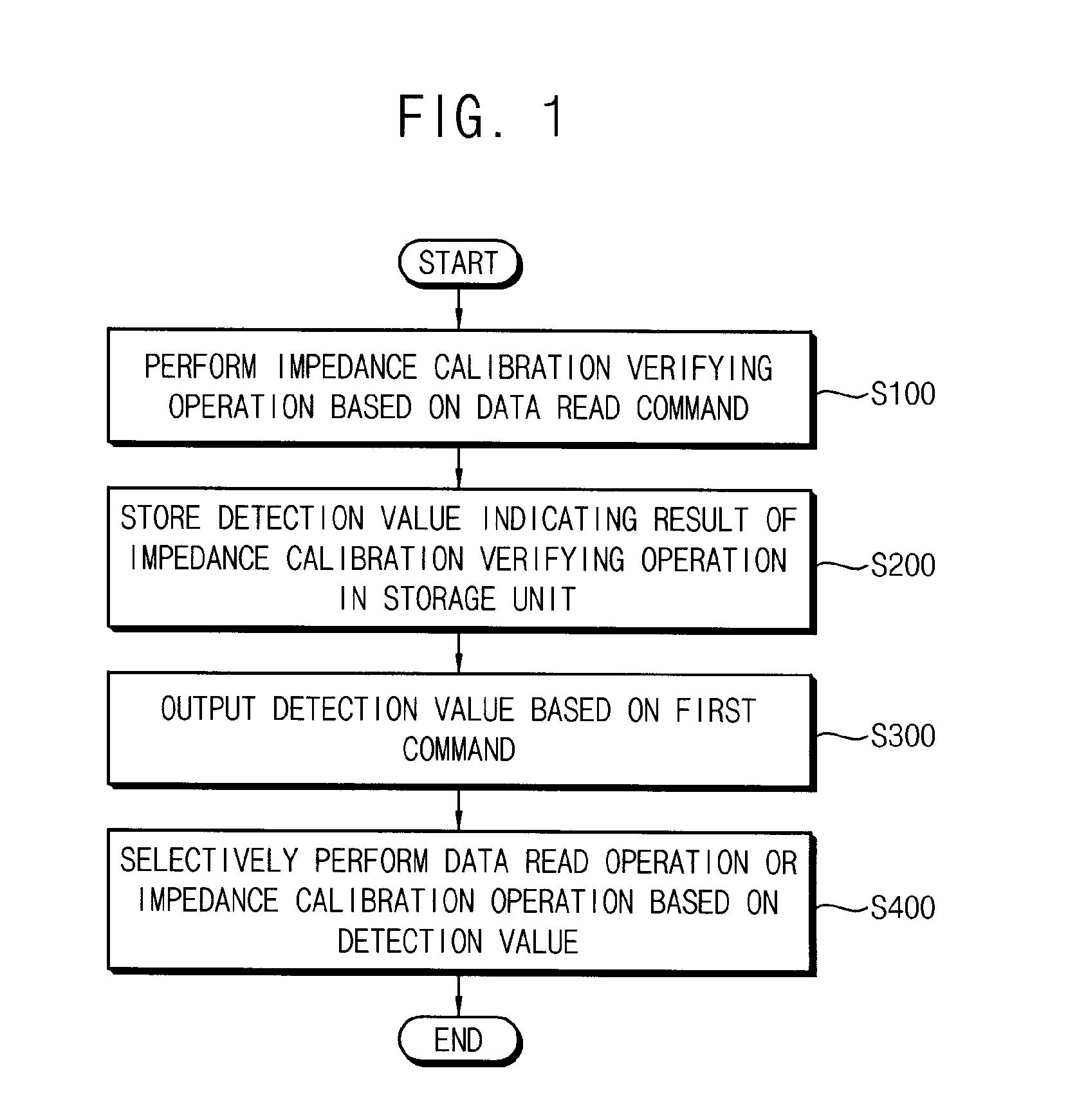
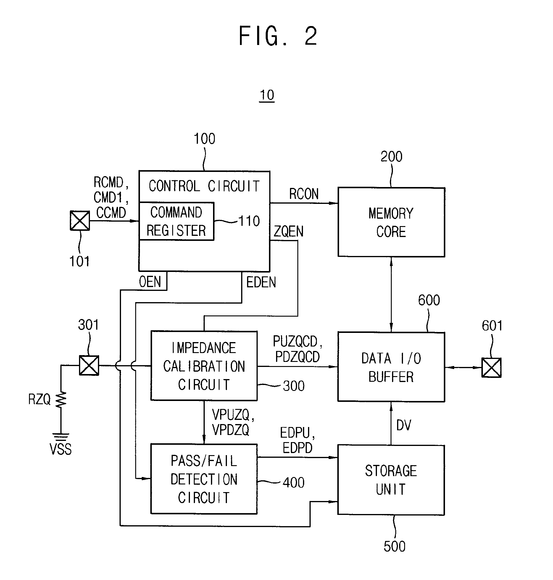
In a method of operating a nonvolatile memory device, an impedance calibration verifying operation is performed based on a data read command. The impedance calibration verifying operation ascertains whether an impedance calibration operation is normally performed for a data input / output (I / O) terminal of the nonvolatile memory device. A detection value is stored in a storage unit. The detection value indicates a result of the impedance calibration verifying operation. The detection value is output based on a first command received after the nonvolatile memory device receives the data read command. A data read operation or the impedance calibration operation is selectively performed based on the detection value.

Description

CROSS-REFERENCE TO RELATED APPLICATION[0001]This application claims priority under 35 USC §119 to Korean Patent Application No. 2014-0033107, filed on Mar. 21, 2014 in the Korean Intellectual Property Office (KIPO), the contents of which are herein incorporated by reference in their entirety.BACKGROUND[0002]1. Technical Field[0003]Example embodiments relate generally to semiconductor memory devices, and to methods of operating nonvolatile memory devices.[0004]2. Description of the Related Art[0005]As the operating speed of a semiconductor memory device has increased, swing widths of signals interfaced between the semiconductor memory device and a memory controller have decreased. A reason for the decrease of the swing widths is to minimize the time required to transmit the signals. However, as the swing widths have decreased, the signals transferred between the semiconductor memory device and the memory controller may be more easily distorted by impedance mismatches caused by proces...

Claims


Application Information

Patent Timeline
IPC IPC(8): G11C16/34G11C16/26
CPCG11C16/26G11C16/3459G11C16/0416G11C16/0483G11C29/022G11C29/028G11C29/1201G11C29/50008
Inventor KANG, KYOUNG-TAE
Owner SAMSUNG ELECTRONICS CO LTD
Learn More