Antenna module and method for manufacturing the same

a technology of anantenna modules and manufacturing methods, applied in the field of anantenna modules, can solve the problems of terahertz oscillation detection devices that cannot be used well as detection devices depending on frequency bands, and the transmission characteristics of signal sg may be largely deteriorated, so as to achieve the effect of suppressing the deterioration of the transmission characteristics of signal sg in a desired frequency band

Active Publication Date: 2015-09-24
NITTO DENKO CORP
View PDF18 Cites 5 Cited by
  • Summary
  • Abstract
  • Description
  • Claims
  • Application Information

AI Technical Summary

Benefits of technology

[0007]An object of the present invention is to provide an antenna module in which deterioration of the transmission characteristics in a desired frequency band is suppressed, and a method for manufacturing the antenna module.
[0013]The above-mentioned configuration blocks the signal that is output from the semiconductor device to propagate from the first and second device connection portions to the first and second antenna portions with the first and the second slits. Thus, the interference with the signal occurs only at the first and second device connection portions. Therefore, the frequency band in which the transmission characteristics are deteriorated can be shifted to a higher region as compared to a case in which the first and second slits are not formed. Further, the position, the width and the shape of the first and second slits are adjusted, whereby the frequency band in which the transmission characteristics are deteriorated can be adjusted. As a result, deterioration of the transmission characteristics at a desired frequency band can be suppressed.
[0014](2) The first and second slits may be formed to be symmetrical with respect to a central axis of the opening. In this case, the directivity of the antenna module is improved.
[0016]In this case, the frequency band in which the transmission characteristics are deteriorated can be shifted to a sufficiently higher region as compared to a case in which the first and second slits are not formed. Thus, deterioration of the transmission characteristics in an even higher frequency band can be suppressed.
[0025](8) The base layer may be a dielectric film made of resin. In this case, the effective relative permittivity of the surroundings of the electrode is reduced. Thus, the electromagnetic wave radiated from the electrode or the electromagnetic wave received by the electrode are less likely attracted to the dielectric film. Therefore, the antenna module can efficiently radiate the electromagnetic wave, and the directivity of the antenna module is improved. Further, the transmission loss of the electromagnetic wave is reduced, and the transmission speed and the transmission distance can be improved.
[0029]Such configuration blocks the signal that is output from the semiconductor device to propagate from the first and second device connection portions to the first and second antenna portions with the first and second slits. Thus, the interference with the signal occurs only at the first and second device connection portions. Therefore, the frequency band in which the transmission characteristics are deteriorated can be shifted to a higher region as compared to a case in which the first and second slits are not formed. Further, the position, the width and the shape of the first and second slits are adjusted, whereby the frequency band in which the transmission characteristics are deteriorated can be adjusted. As a result, deterioration of the transmission characteristics in a desired frequency band can be suppressed.

Problems solved by technology

In a case in which the above-mentioned terahertz oscillation detection device operates as the detection device, the transmission characteristics may be largely deteriorated at the time of receiving the electromagnetic wave in a specific frequency band.
Therefore, the terahertz oscillation detection device cannot be used well as the detection device depending on the frequency band of the used electromagnetic wave.

Method used


Image

  • Antenna module and method for manufacturing the same
  • Antenna module and method for manufacturing the same
  • Antenna module and method for manufacturing the same

Examples


first embodiment

(1) First Embodiment

(1-1) Configuration of Antenna Module

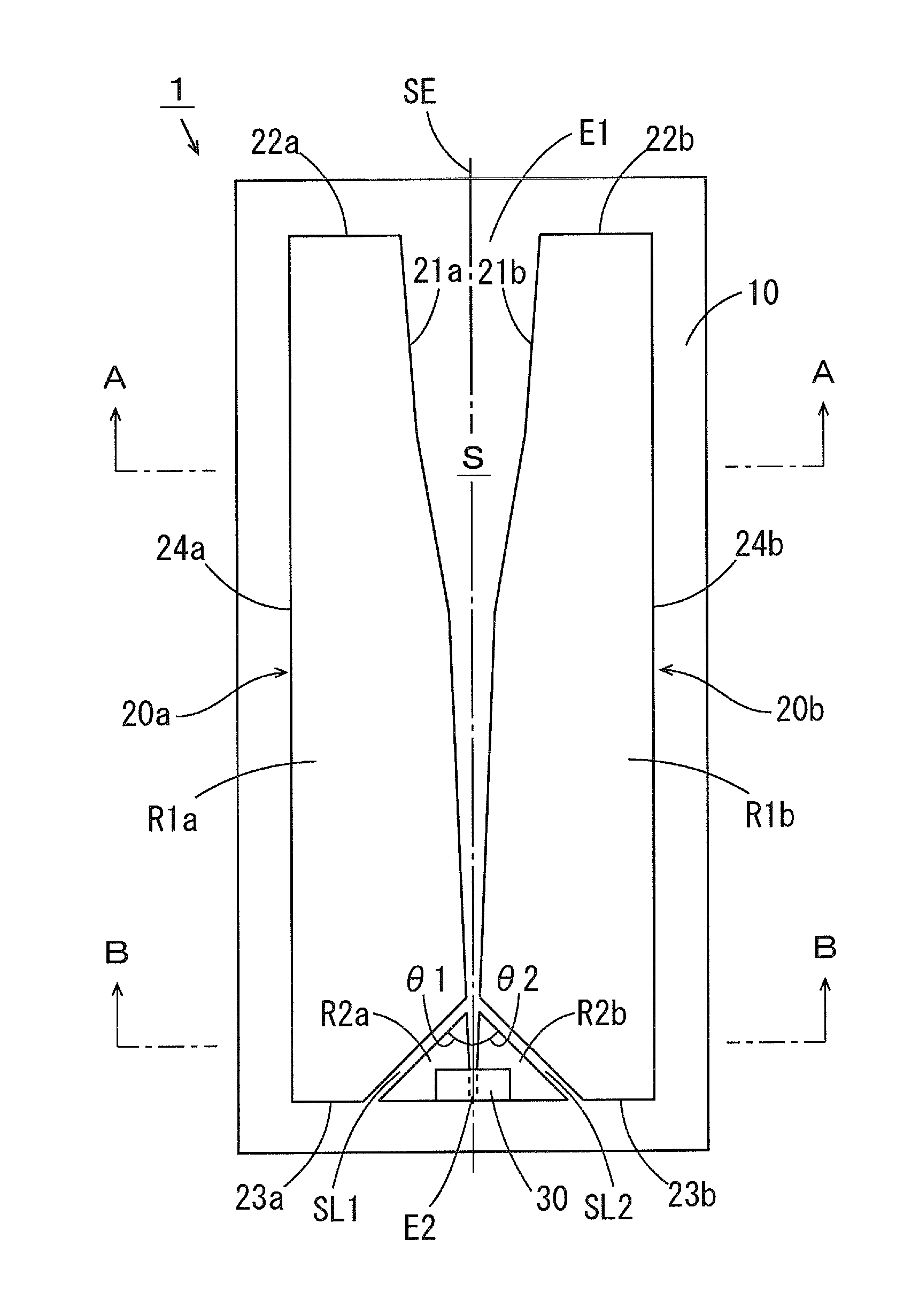
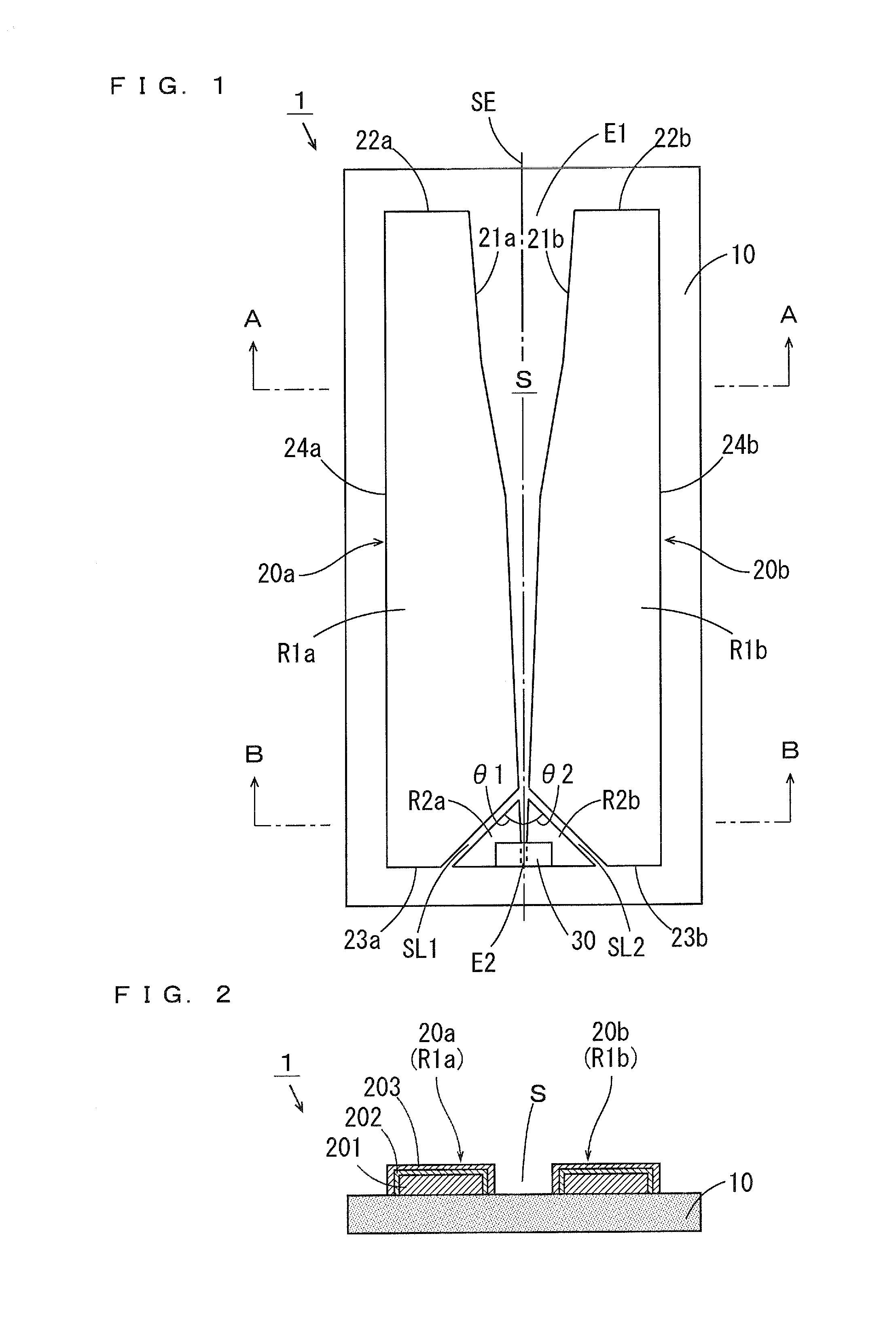
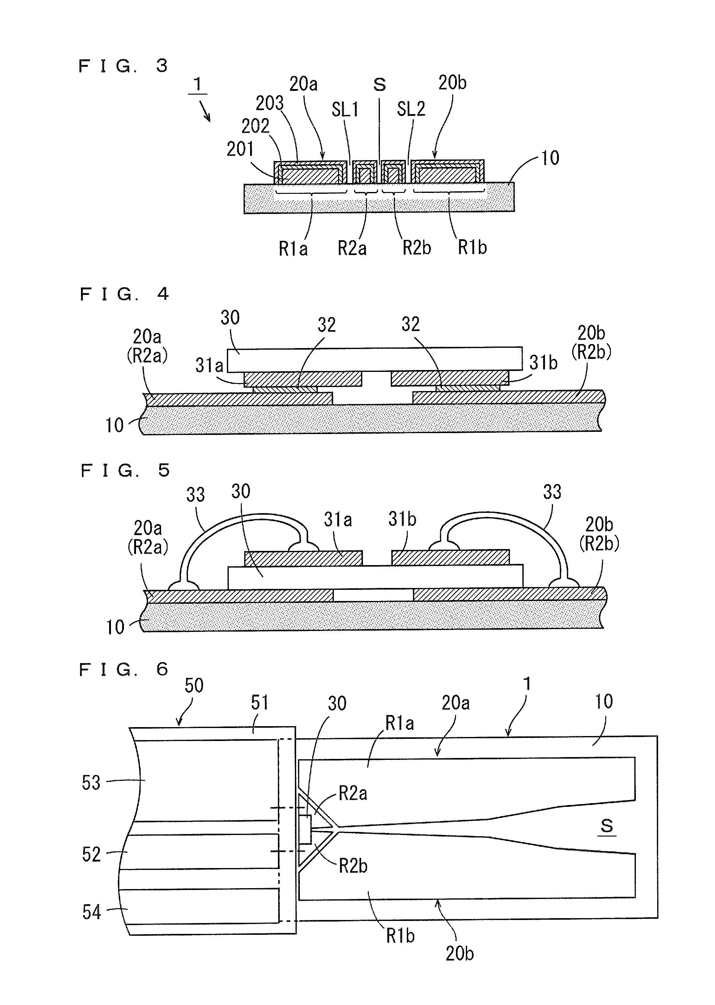
[0072]FIG. 1 is a schematic plan view of the antenna module according to the first embodiment of the present invention. FIG. 2 is a schematic cross sectional view taken along the line A-A of the antenna module of FIG. 1. FIG. 3 is a schematic cross sectional view taken along the line B-B of the antenna module of FIG. 1.

[0073]In FIG. 1, the antenna module 1 is constituted by a base layer 10, a pair of electrodes 20a, 20b and a semiconductor device 30. The base layer 10 is made of an insulative material. One surface of the two surfaces of the base layer 10 opposite to each other is referred to as a main surface, and the other surface is referred to as a back surface. In the present embodiment, the main surface is an example of a first surface, and the back surface is an example of a second surface.

[0074]The pair of electrodes 20a, 20b is formed on the main surface of the base layer 10. A gap that extends from one end to the othe...

second embodiment

(2) Second Embodiment

[0147]FIG. 23 is a schematic plan view of the antenna module 1 according to the second embodiment of the present invention. Regarding the antenna module 1 of FIG. 23, difference from the antenna module 1 according to the above-mentioned first embodiment will be described.

[0148]In the antenna module 1 of FIG. 23, the slits SL1, SL2 are formed at the electrodes 20a, 20b to respectively extend on a common straight line vertical to the central axis SE of the tapered slot S.

(2-1) Characterization of Antenna Module

[0149]Characteristics of the antenna module 1 according to the second embodiment was evaluated by the simulation.

(a) INVENTIVE EXAMPLES 6 TO 12

[0150]Except that the slits SL1, SL2 are formed as shown in FIG. 23, the antenna module 1 of the inventive examples 6 to 12 has the same configuration as the antenna module 1 of the inventive example 1, and is connected to the circuit board 50 by the wire connection similarly to the antenna module 1 of the inventive e...

third embodiment

(3) Third Embodiment

[0163]FIG. 29 is a schematic plan view of the antenna module 1 according to the third embodiment of the present invention. Regarding the antenna module 1 of FIG. 29, difference from the antenna module 1 according to the above-mentioned first embodiment will be described.

[0164]In the antenna module 1 of FIG. 29, the slits SL1, SL2 are provided to respectively extend in a curved line from the side surfaces 21a, 21b to the end surfaces 23a, 23b of the electrodes 20a, 20b. The slits SL1, SL2 are formed to be symmetrical with each other with respect to the central axis SE of the tapered slot S. Further, the slits SL1, SL2 are respectively formed to extend along a circle with the mount end E2 used as a center.

(3-1) Characterization of Antenna Module

[0165]The characteristics of the antenna module 1 according to the third embodiment were evaluated by the simulation.

(a) INVENTIVE EXAMPLES 13 TO 16

[0166]Except that the slits SL1, SL2 are formed as shown in FIG. 29, the ant...


PUM


Abstract

First and second conductor layers are formed on a main surface of a base layer. A tapered slot is formed between the first and second conductive layers. A first slit is formed at the first conductor layer, and a second slit is formed at the second conductor layer. Thus, the first conductor layer is divided into a first device connection portion and a first antenna portion, and the second conductor layer is divided into a second device connection portion and a second antenna portion. A semiconductor device is connected to the first and second device connection portions.

Description

BACKGROUND OF THE INVENTION[0001]1 Field of the Invention[0002]The present invention relates to an antenna module that transmits or receives an electromagnetic wave of a frequency in a terahertz band not less than 0.05 THz and not more than 10 THz, for example, and a method for manufacturing the antenna module.[0003]2. Description of Related Art[0004]Terahertz transmission using an electromagnetic wave in the terahertz band is expected to be applied to various purposes such as short-range super high speed communication and uncompressed delayless super high-definition video transmission.[0005]A terahertz oscillation detection device using a semiconductor substrate is described in JP 2013-5115 A. In the terahertz oscillation detection device described in JP 2013-5115 A, first and second electrodes, an MIM (Metal Insulator Metal) reflector, a resonator and an active element are formed on the semiconductor substrate. A horn opening is arranged between the first electrode and the second ...

Claims


Application Information

Patent Timeline
Patent Type & Authority Applications(United States)
IPC IPC(8): H01Q13/10H01L21/768H01L23/66H01Q23/00H01L23/12H01L23/528
CPCH01Q13/106H01L23/12H01L21/76892H01L23/66H01Q23/00H01L23/528H01Q1/248H01Q1/52H01Q13/085H01L2224/16225H01L2224/48091H01L2224/48464H01L2924/00014
Inventor INOUE, MASAMIHODONO, MASAYUKIHONJO, MITSURU
Owner NITTO DENKO CORP
Why Eureka
Try Eureka