Method of producing optical device, optical device, optical system, and imaging device

Active Publication Date: 2015-10-01
ASAHI GLASS CO LTD
View PDF3 Cites 7 Cited by
  • Summary
  • Abstract
  • Description
  • Claims
  • Application Information

AI Technical Summary

Benefits of technology

[0009]According to an aspect of the present invention, an optical device includes a light absorbing part made of a material that absorbs a part or an entirety of light and formed on a base material; and a light transmitting part made of a material that transmits the light and formed on the light absorbing part, wherein a center region, an intermediate region, and a peripheral region are concentrically formed from a center toward a periphery of the optical device, the light absorbing part is substantially absent in the center region, a thickness of the light absorbing part gradually increases in a direction from the center region to the peripheral region in the intermediate region, and 0.3<φ1/φ2<0.9 is satisfied where φ1 is a diameter of a boundary between the center region and the intermediate region and φ2 is a diameter of a boundary between the intermediate region and the perip

Problems solved by technology

When the diaphragm 910 is reduced in size, however, the diffraction of light occurs to a n

Method used


Image

  • Method of producing optical device, optical device, optical system, and imaging device
  • Method of producing optical device, optical device, optical system, and imaging device
  • Method of producing optical device, optical device, optical system, and imaging device

Examples


Example

First Embodiment

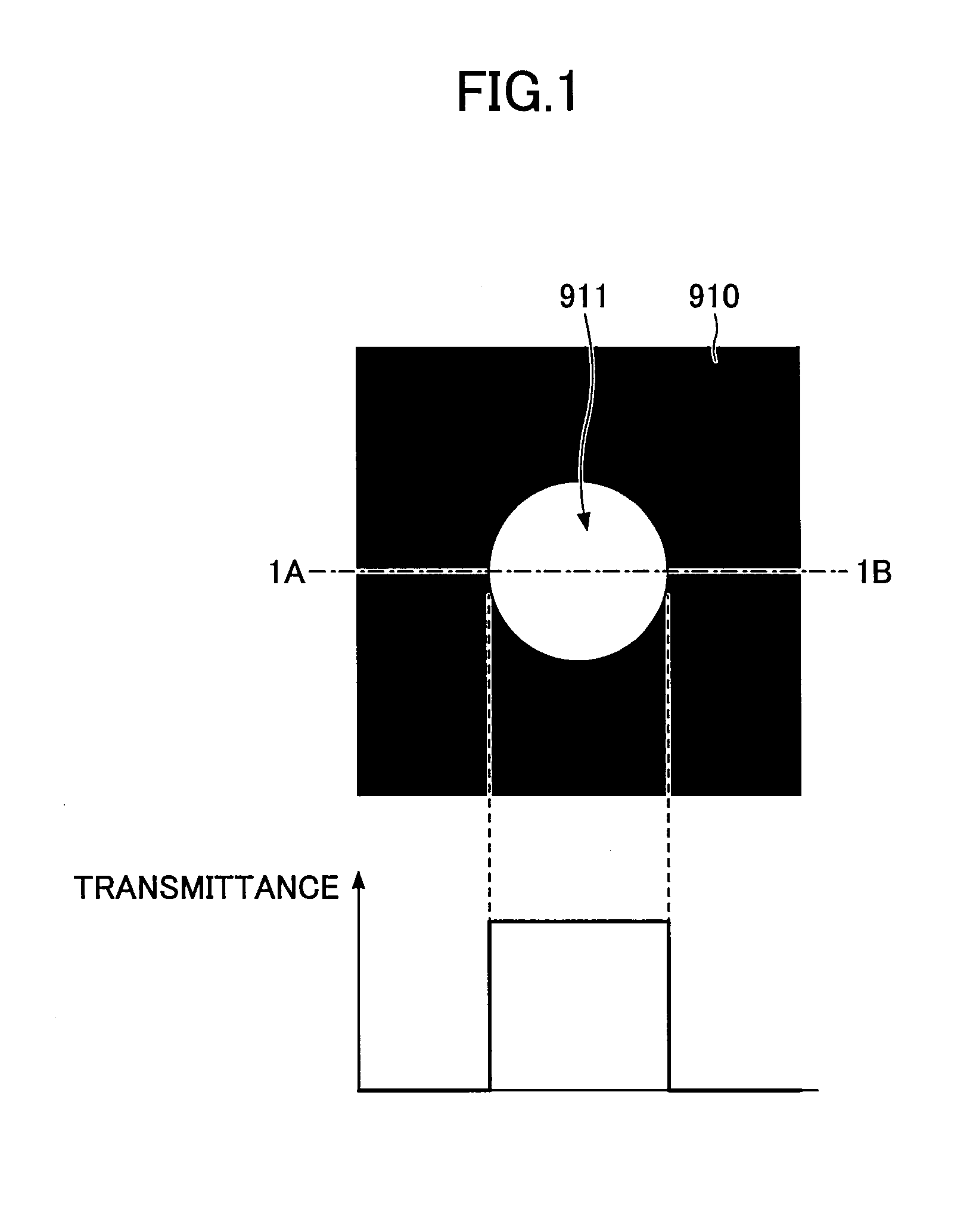
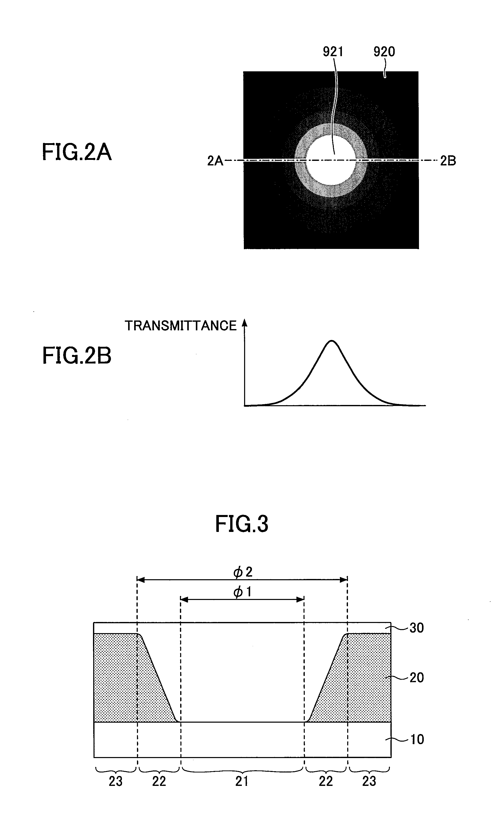
[0031]A description is given of an optical device according to a first embodiment. The optical device according to this embodiment is a so-called “apodization filter.” Referring to FIGS. 3, 4A and 4B, the optical device includes a transparent base material (substrate) 10 and a light absorbing part 20 and a light transmitting part 30 formed on the transparent base material 10. The transparent base material 10 is formed of a transparent resin material or glass. The light absorbing part 20 is formed of a material that absorbs visible light. The light transmitting part 30 is formed of a material that transmits visible light (a light transparent material). FIG. 4A is a plan view of the optical device according to this embodiment, and FIG. 4B illustrates a light transmittance distribution along one-dot chain line 4A-4B of FIG. 4A.

[0032]The optical device according to this embodiment includes a center region 21 at the center of the optical device, an intermediate region 22 ...

Example

Second Embodiment

[0058]Next, a description is given of a second embodiment. This embodiment is directed to a method of producing the optical device of the first embodiment. A description is given, with reference to FIGS. 6A through 6F, of a production method of this embodiment, according to which multiple optical devices according to the first embodiment are simultaneously produced.

[0059]Referring to FIG. 6A, first, an appropriate amount of the light absorbing resin material 20a for forming the light absorbing part 20 is dropped onto the transparent base material 10. The light absorbing resin material 20a is a liquid in which an absorbing material is added to a transparent resin material. The light absorbing resin material 20a used in this embodiment is cured through exposure to ultraviolet radiation.

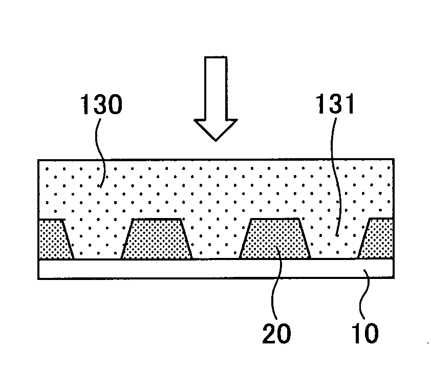
[0060]Next, referring to FIG. 6B, a forming mold 130 having an uneven surface on which irregularities corresponding to the shape of the light absorbing part 20 to be formed is faulted i...

Example

Third Embodiment

[0075]Next, a description is given of a third embodiment. This embodiment is directed to a method of producing the optical device of the first embodiment. A description is given, with reference to FIGS. 8A through 8G, of a production method of this embodiment, according to which multiple optical devices according to the first embodiment are simultaneously produced.

[0076]Referring to FIG. 8A, first, an appropriate amount of the light absorbing resin material 20a for forming the light absorbing part 20 is dropped onto the transparent base material 10. The light absorbing resin material 20a is a liquid in which an absorbing material is added to a transparent resin material. The light absorbing resin material 20a is cured through exposure to ultraviolet radiation.

[0077]Next, referring to FIG. 8B, the light absorbing resin material 20a is exposed to ultraviolet radiation. As a result, light absorbing resin material 20a is cured, so that a light absorbing material part 20b...


PUM

PropertyMeasurementUnit
Lengthaaaaaaaaaa
Transparencyaaaaaaaaaa
Lightaaaaaaaaaa

Abstract

A method of producing an optical device, which includes a center region where a light absorbing part is substantially absent, a peripheral region, and an intermediate region between the center and peripheral regions, where the thickness of the light absorbing part gradually increases in a direction from the center region to the peripheral region, includes applying a resin material that absorbs light onto a transparent base material. A forming mold including a convex and a concave corresponding to the shape of the light absorbing part is pressed against the applied resin material. The light absorbing part is formed by curing the resin material through exposure to ultraviolet radiation with the forming mold being pressed against the resin material. A surface of the convex that faces the resin material when the forming mold is pressed against the resin material corresponds to the center region of the optical device and is flat.

Description

CROSS-REFERENCE TO RELATED APPLICATIONS[0001]The present application is a continuation application filed under 35 U.S.C. 111(a) claiming benefit under 35 U.S.C. 120 and 365(c) of PCT International Application No. PCT / JP2013 / 083791, filed on Dec. 17, 2013 and designating the U.S., which claims priority to Japanese Patent Application No. 2012-279101, filed on Dec. 21, 2012. The entire contents of the foregoing applications are incorporated herein by reference.BACKGROUND OF THE INVENTION[0002]1. Field of the Invention[0003]The present invention relates to methods of producing an optical device, optical devices, optical systems, and imaging devices.[0004]2. Description of the Related Art[0005]In optical instruments such as cameras, an optical diaphragm and a neutral density (ND) filter are used in order to control the amount of light that enters a lens. Cellular phones and mobile terminals also are equipped with a camera, and such a camera uses an optical diaphragm (for example, Japanes...

Claims


Application Information

Patent Timeline
IPC IPC(8): G02B5/00G01J1/04G02B13/00
CPCG02B5/003G01J1/0488G02B13/001G02B1/04C08L33/08
Inventor NOMURA, TAKUJI
Owner ASAHI GLASS CO LTD
Why Eureka
Try Eureka