Device and method for printing a thixotropic medium onto a PCB

Inactive Publication Date: 2015-10-08
ASM ASSEMBLY SYST SINGAPORE PTE LTD
View PDF11 Cites 10 Cited by
  • Summary
  • Abstract
  • Description
  • Claims
  • Application Information

AI Technical Summary

Benefits of technology

[0006]It is an object of the present invention to overcome the aforesaid disadvantages. In particular it is an aim of the present invention to provide a device and a method for printin

Problems solved by technology

Nevertheless, the thixotropic characteristic of the solder paste represents a problem if the time elapsed between the printing of two successive PCBs on a printing line using the same printing head is too long and thus the solder paste within the printing head transforms into a state of relatively high viscosity.
This may have a negative effect on the printing quality of the second PCB.
Usually the timing between printing of two successive PCBs on a printing line is short enough to avoid transformation

Method used


Image

  • Device and method for printing a thixotropic medium onto a PCB
  • Device and method for printing a thixotropic medium onto a PCB
  • Device and method for printing a thixotropic medium onto a PCB

Examples


Embodiment Construction

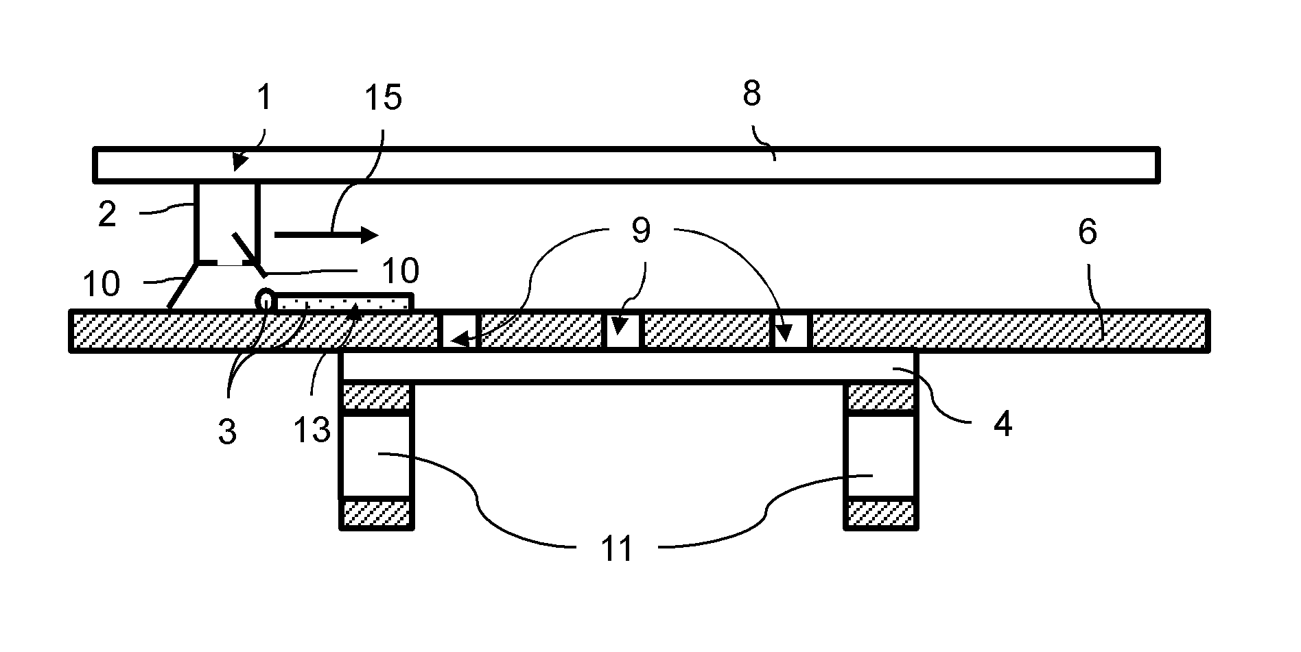
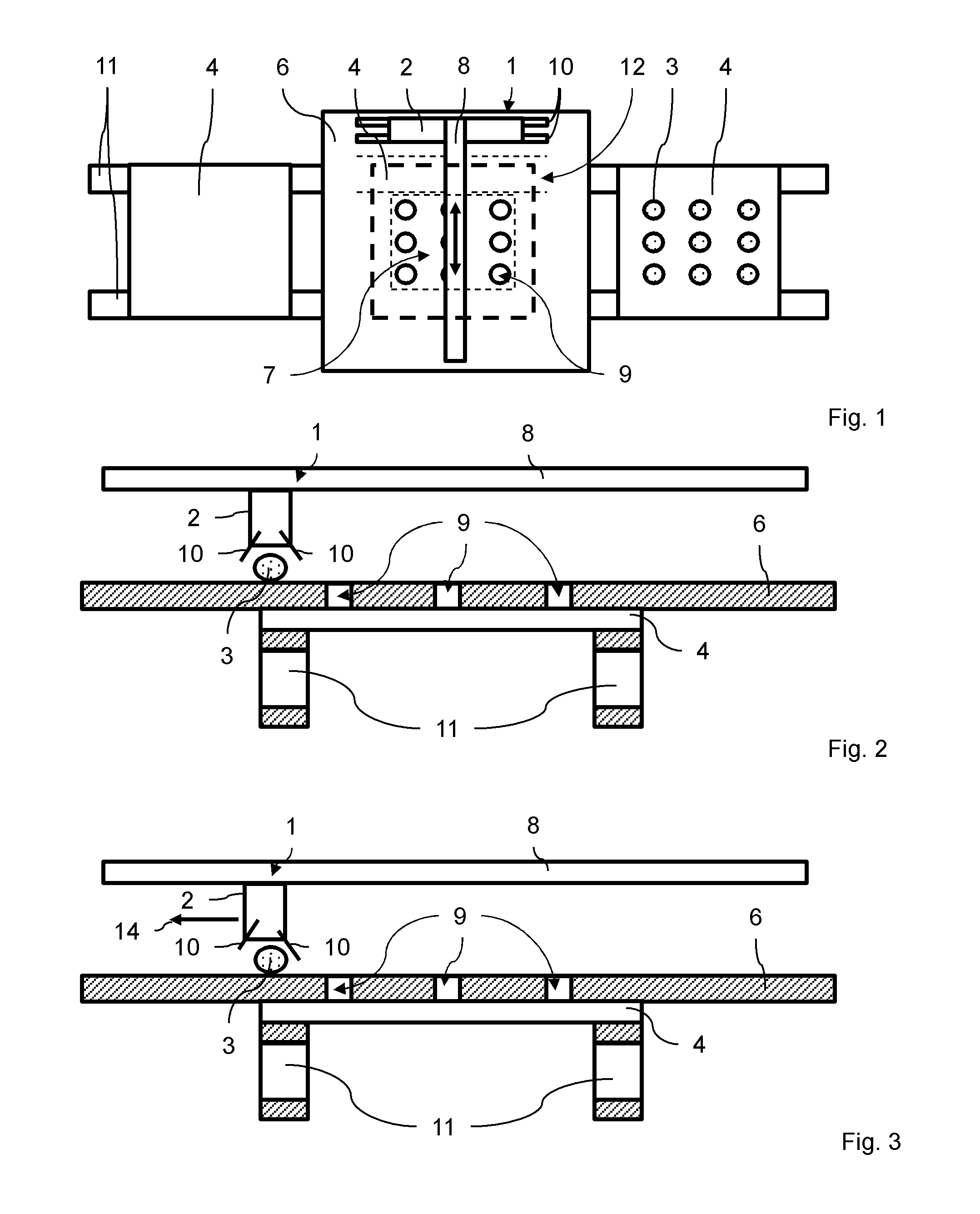
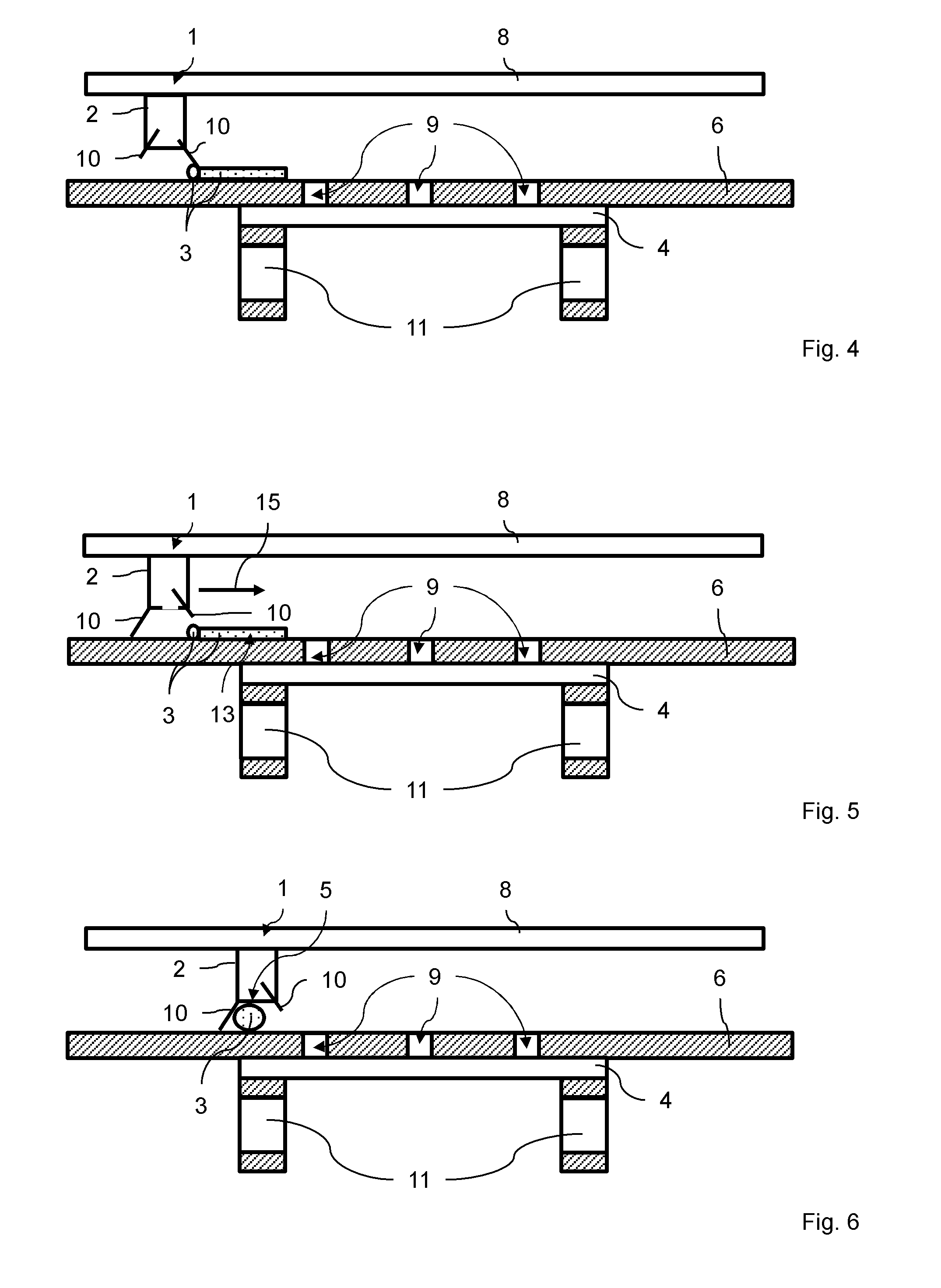
[0019]The printing device according to FIG. 1 is integrated into a printing line and comprises a printing head 1 including extractable squeegees 10. The squeegees 10 are held by a printing head base 2 which may incorporate actuators (not shown) for extending and retracting the squeegees 10. The PCBs 4, onto which the solder paste 3 is to be applied successively, are already provided with printed conductors (not shown). In a process following the application of the solder paste 3, electronic components such as resistors, capacitors, etc. (not shown) are soldered to respective contact areas of the PCBs 4. Applying discrete amounts of the solder paste 3 onto those contact areas of the PCBs 4 by means of the printing device, in particular the printing head 1, represents thus a first step in the soldering of the electronic components to the PCBs 4.

[0020]Applying the solder paste 3 onto the contact areas of the PCBs 4 is done in a conventional manner by dispensing a discrete amount of the...


PUM

PropertyMeasurementUnit
Timeaaaaaaaaaa
Surface areaaaaaaaaaaa
Thixotropic indexaaaaaaaaaa

Abstract

A device for printing a thixotropic medium onto a PCB comprising a printing head adapted to apply the thixotropic medium to a surface of the PCB is characterized in that the device further comprises a surface area where the thixotropic medium is locatable to be repeatably worked upon in a kneading operation during which at least a part of the thixotropic medium is kneaded while the printing head is not in use for applying the thixotropic medium onto the PCB.

Description

FIELD OF THE INVENTION[0001]The present invention relates to a device for printing a thixotropic medium, such as a solder paste, onto a printed circuit board (PCB), the device comprising a printing head adapted to apply the thixotropic medium to a surface of the PCB. The invention relates further to a method for printing a thixotropic medium, such as a solder paste, onto a PCB using such a printing head.BACKGROUND AND PRIOR ART[0002]An example of a printing device being adapted for applying a print medium such as a solder paste onto selected areas of a PCB using a screen is disclosed in US patent publication number 2010 / 0139509 A1.[0003]The printing device disclosed therein comprises a printing head, which can be driven in a reciprocal movement within a support during a printing operation. The printing head comprises a delivery aperture through which the solder paste is delivered from a cavity, in which the solder paste is stored. A rotatable unit is positioned within the cavity, wh...

Claims


Application Information

Patent Timeline
IPC IPC(8): B23K3/06B23K31/02B23K37/00B23K1/00B23K1/20
CPCB23K3/0638B23K1/0016B23K2201/42B23K37/00B23K31/02B23K1/20H05K3/1233H05K3/3485
Inventor GRAY, ROBERTPARDAVE, GABRIEL DE JESUS
Owner ASM ASSEMBLY SYST SINGAPORE PTE LTD
Why Eureka
Try Eureka