Optical device including three-coupled quantum well structure

Active Publication Date: 2015-10-08
SAMSUNG ELECTRONICS CO LTD +1
View PDF1 Cites 7 Cited by
  • Summary
  • Abstract
  • Description
  • Claims
  • Application Information

AI Technical Summary

Benefits of technology

This patent relates to a device that uses a three-coupled quantum well structure to improve the absorption of light without increasing the driving voltage. The technical effect of this invention is to enhance the performance of optical devices by improving their ability to absorb light.

Problems solved by technology

Thus, since a high absorption intensity and a low driving voltage are in a trade-off relationship, it is difficult to simultaneously achieve improvement of the absorption intensity and reduction of the driving voltage.
Since a GaAs substrate is not transparent with respect to the 850 nm wavelength light, a complicated process of removing the GaAs substrate is added to the process of manufacturing an optical modulator.
However, since a lattice constant of the material of a quantum well layer and a barrier suitable for an optical modulator having a 940 nm resonance wavelength does not match the resonance wavelength of the GaAs substrate, stress and strain may be generated.
Unless the stress and strain are compensated, quantum wells of a large number of layers are not stacked and thus it is difficult to increase the absorption intensity of an optical modulator.

Method used


Image

  • Optical device including three-coupled quantum well structure
  • Optical device including three-coupled quantum well structure
  • Optical device including three-coupled quantum well structure

Examples


Embodiment Construction

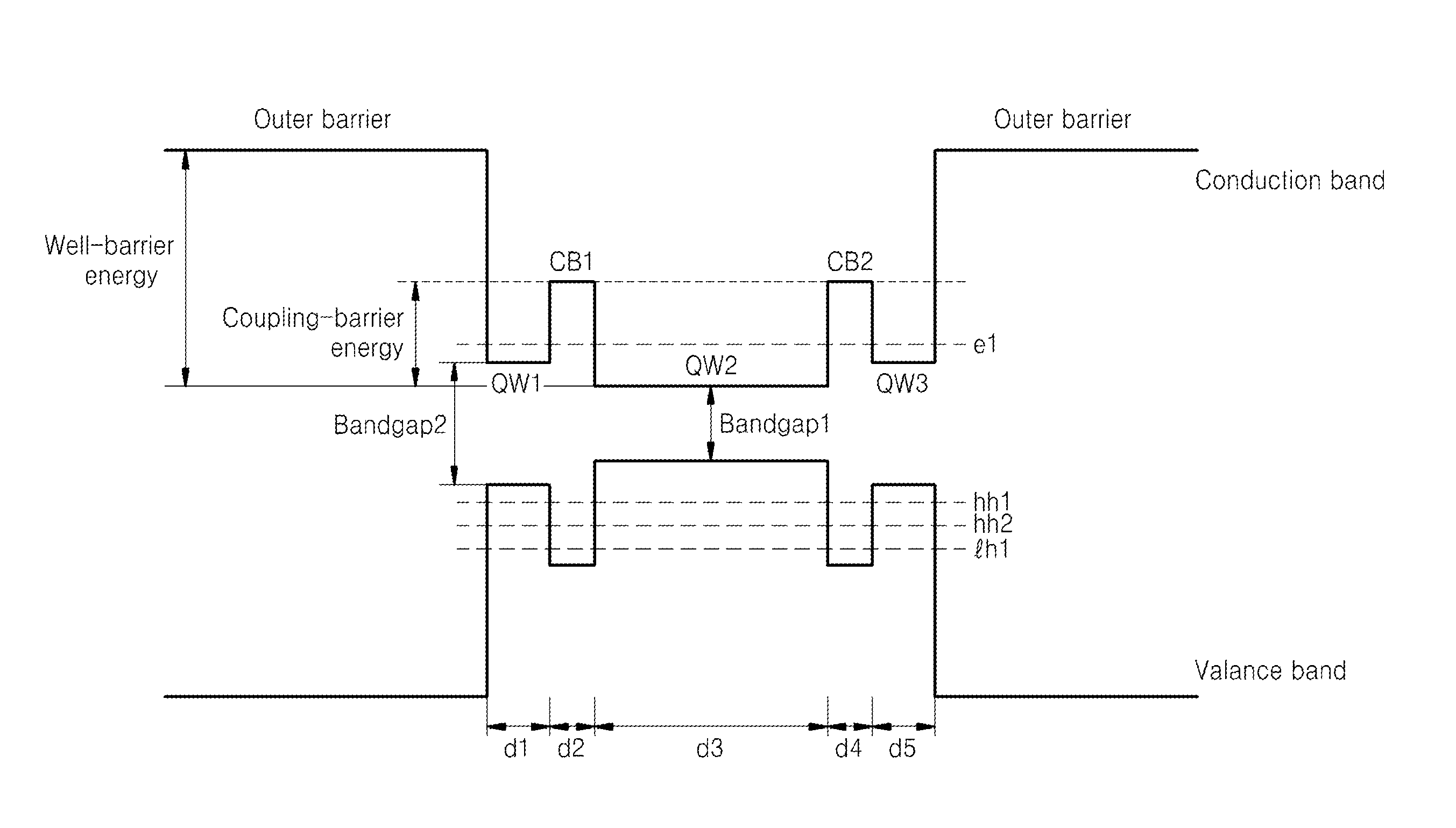
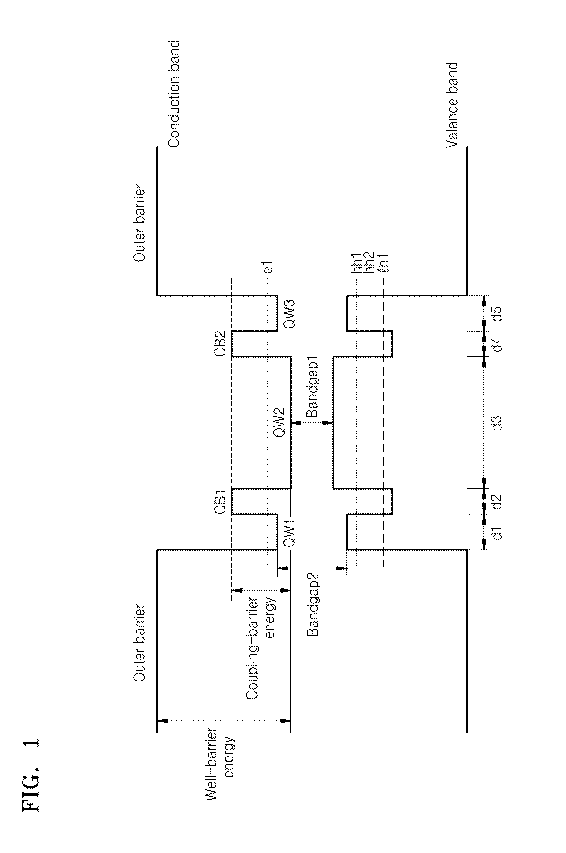
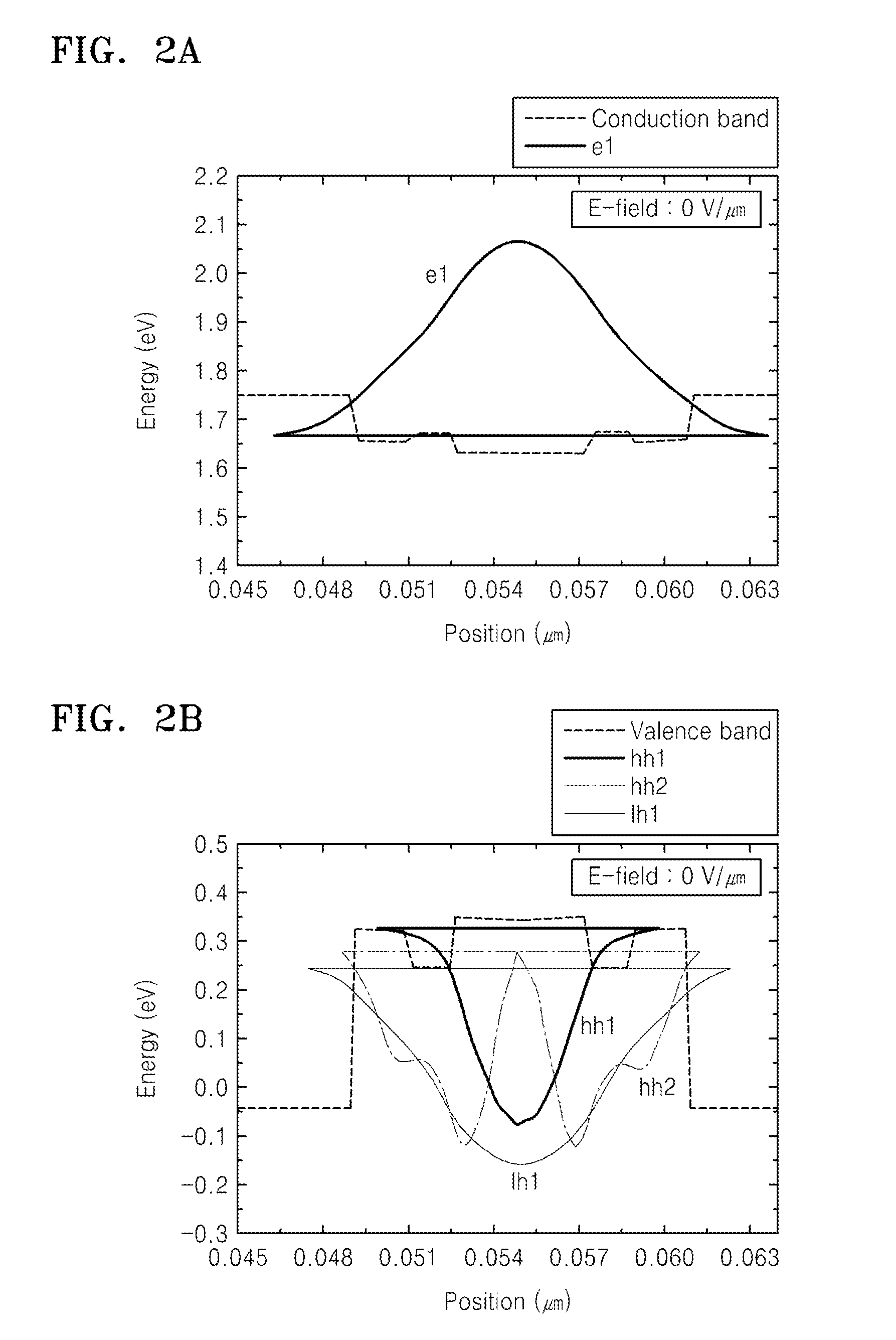
[0055]Reference will now be made in detail to an optical device including a three-coupled quantum well structure, examples of which are illustrated in the accompanying drawings, wherein like reference numerals refer to like elements throughout. Also, the size of each layer illustrated in the drawings may be exaggerated for convenience of explanation and clarity. In this regard, the example embodiments may have different forms and should not be construed as being limited to the descriptions set forth herein. Accordingly, the example embodiments are merely described below, by referring to the figures, to explain the example description.

[0056]It will be understood that when an element is referred to as being “on,”“connected” or “coupled” to another element, it can be directly on, connected or coupled to the other element or intervening elements may be present. In contrast, when an element is referred to as being “directly on,”“directly connected” or “directly coupled” to another elemen...


PUM


Abstract

An optical device includes an active layer that includes at least two outer barriers and at least one coupled quantum well that is inserted between the at least two outer barriers. Each coupled quantum well includes at least three quantum well layers and at least two coupling barriers that are respectively provided between the at least three quantum well layers. Thicknesses of two quantum well layers disposed at opposite end portions of the at least three quantum well layers are less than a thickness of the other quantum well layer disposed between the two quantum well layers disposed at the opposite end portions. A bandgap of the two quantum well layers disposed at the opposite end portions may be higher than a bandgap of the other quantum well layer disposed between the two quantum well layers.

Description

RELATED APPLICATIONS[0001]This application claims priority from Korean Patent Application No. 10-2014-0040746, filed on Apr. 4, 2014, in the Korean Intellectual Property Office, the disclosure of which is incorporated herein in its entirety by reference.BACKGROUND[0002]1. Field[0003]Example embodiments relate to an optical device including a three-coupled quantum well structure, and / or to an optical device including a three-coupled quantum well structure, which may improve the light absorption intensity in a multiple quantum well structure without increasing a driving voltage.[0004]2. Description of the Related Art[0005]3D cameras typically have not only a general image capturing function, but also a function of measuring a distance from a plurality of points on a surface of an object. A variety of algorithms for measuring the distance between an object and a 3D camera have recently been suggested. A typical algorithm is a time-of-flight (TOF) algorithm. According to the TOF algorit...

Claims


Application Information

Patent Timeline
IPC IPC(8): G02F1/017
CPCG02F2001/0175G02F2001/0157G02F1/01725G02F2001/01733B82Y20/00G02F2001/01766Y10S977/755G02F1/01733G02F1/01766H01L31/035236H01L31/075H01L31/105Y02E10/548G02F1/133605G02F1/0157G02F1/0175H01L23/528H01L23/53223H01L31/00H01L33/04H01L33/10H01L33/42H01L33/46H01L33/502H01L33/58H01L33/60H01L33/62H01L2224/05124H01L2924/00H01L2924/00014H01L2924/12042
Inventor CHO, YONGCHULLEE, YONGTAKNA, BYUNGHOONPARK, CHANGYOUNGJU, GUNWUPARK, YONGHWA
Owner SAMSUNG ELECTRONICS CO LTD
Why Eureka
Try Eureka