Display Device and Electronic Device

a display device and electronic technology, applied in the field of display devices, can solve the problems of reducing reliability and manufacturing yield of the display device, easily damage to the electrode included in the display device, etc., and achieve the effects of high reliability, not easily damaged the display region, and not easily damaged the electrod

Active Publication Date: 2015-10-29
SEMICON ENERGY LAB CO LTD
View PDF22 Cites 37 Cited by
  • Summary
  • Abstract
  • Description
  • Claims
  • Application Information

AI Technical Summary

Benefits of technology

[0024]One embodiment of the present invention can provide a method of manufacturing a display device that does not easily damage an electrode. Another embodiment of the present invention can provide a method of manufacturing a display device that does not easily damage a display region. Another embodiment of the present invention can provide a highly reliable display device and a manufacturing method thereof. Another embodiment of the present invention can provide a display device with high design flexibility and a manufacturing method thereof.
[0025]One embodiment of the present invention provides a display device, electronic device, or the like having high visibility. One embodiment of the present invention provides a display device, electronic device, or the like having high display quality. One embodiment of the present invention provides a display device, electronic device, or the like having high reliability. One embodiment of the present invention provides a display device, electronic device, or the like that is unlikely to be broken. One embodiment of the present invention provides a display device, electronic device, or the like with low power consumption. One embodiment of the present invention provides a display device, electronic device, or the like with high productivity. One embodiment of the present invention provides a novel display device, electronic device, or the like.

Problems solved by technology

However, a method in which part of a flexible substrate is removed by a laser beam or with an edged tool has a problem in that an electrode included in a display device is damaged easily and the reliability and manufacturing yield of the display device are reduced easily.

Method used


Image

  • Display Device and Electronic Device
  • Display Device and Electronic Device
  • Display Device and Electronic Device

Examples


embodiment 1

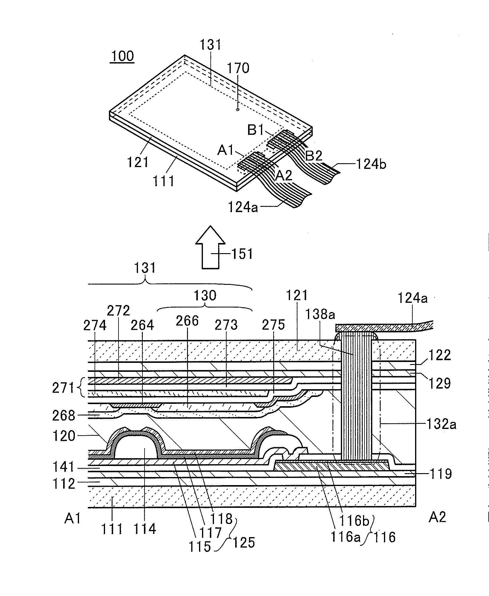
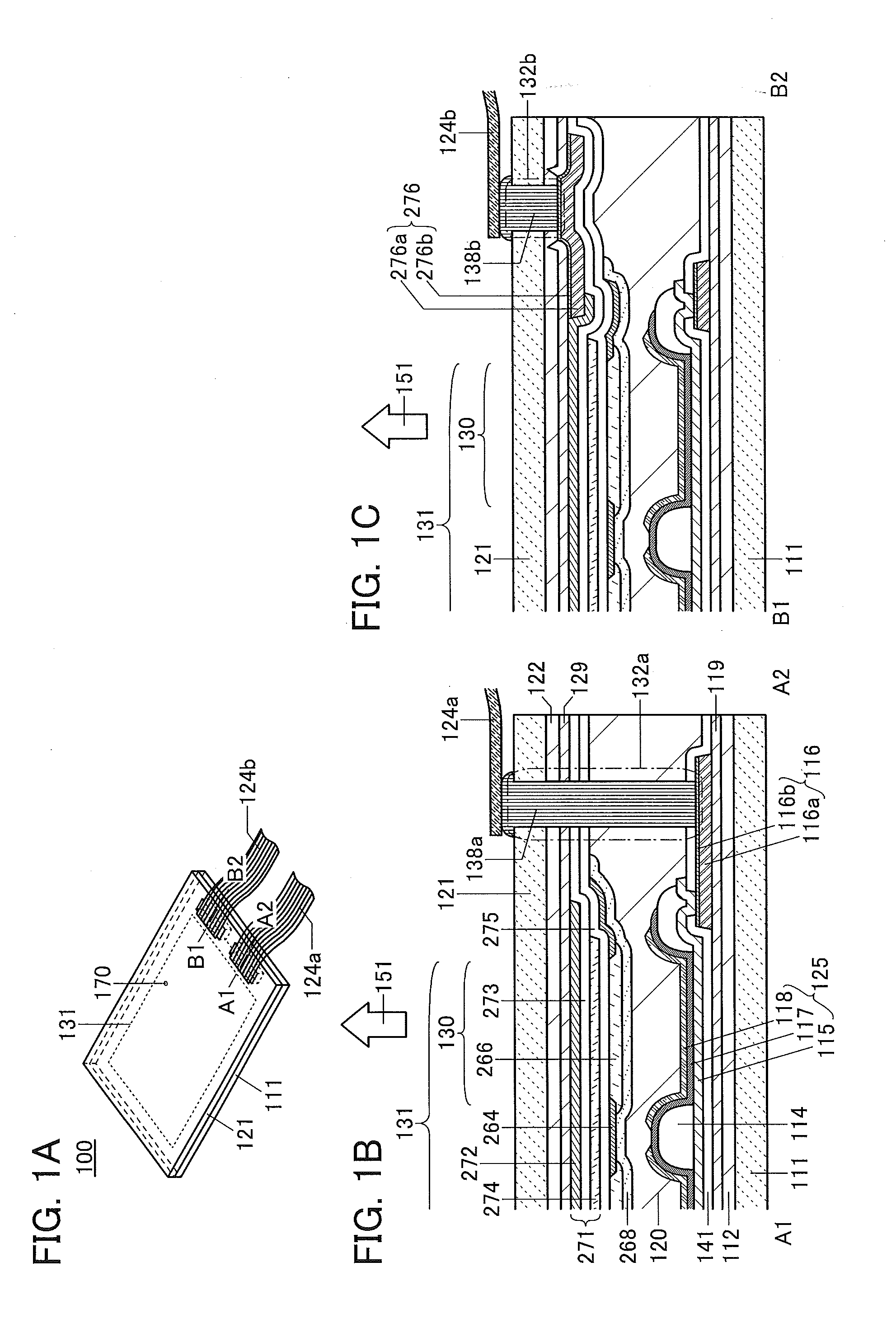
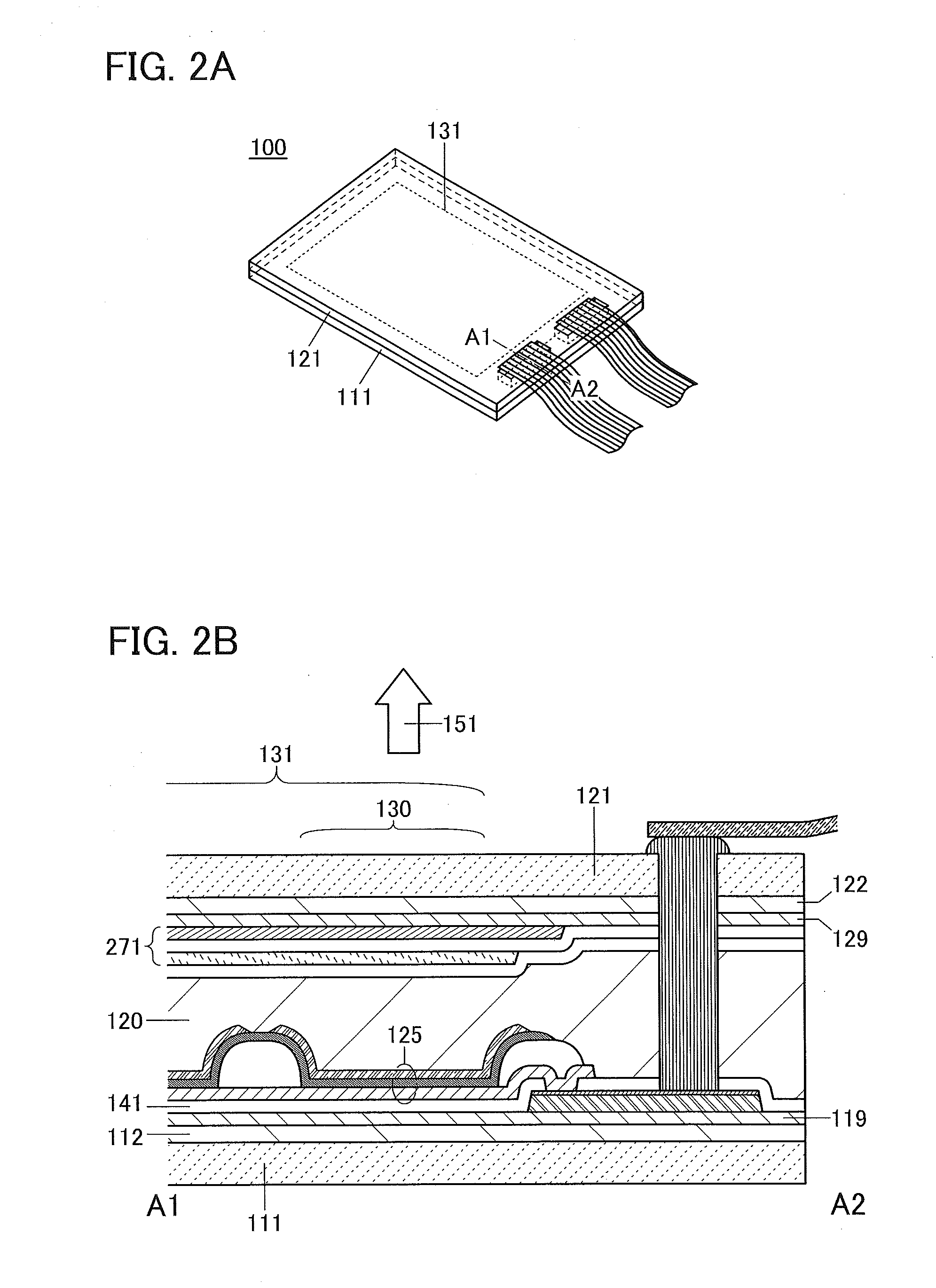
[0094]A structure and a manufacturing method of a display device 100 of one embodiment of the present invention are described with reference to FIGS. 1A to 1C, FIGS. 2A and 2B, FIGS. 3A and 3B, FIGS. 4A to 4E, FIGS. 5A to 5C, FIGS. 6A and 6B, FIGS. 7A to 7D, FIGS. 8A to 8D, FIGS. 9A to 9D, FIGS. 10A to 10C, FIGS. 11A and 11B, FIGS. 12A and 12B, FIGS. 13A and 13B, FIGS. 14A and 14B, FIGS. 15A and 15B, FIGS. 16A and 16B, FIGS. 17A and 17B, FIGS. 18A and 18B, and FIGS. 19A to 19C. Note that the display device 100 disclosed in this specification is a display device in which a light-emitting element is used as a display element. As the display device 100 of one embodiment of the present invention, a display device having a top-emission structure is described as an example. Note that the display device 100 can be a display device having a bottom-emission structure or a dual-emission structure.

[0095]A structure example of the display device 100 of one embodiment of the present invention is...

embodiment 2

[0217]In this embodiment, a display device 1100 having a structure different from the structure of the display device 100 described in the above embodiment is described. In this embodiment, a description is made of portions different from the display device 100 to avoid repetition of the same description.

[0218]The display device 1100 described in this embodiment is different from the display device 100 in connection portions of the external electrodes 124 (the external electrode 124a, external electrode 124b). Specifically, in the display device 100, the external electrode 124 is connected from the substrate 121 side, while in the display device 1100, the external electrode 124 is connected from the substrate 111 side. In addition, the stacking order of the electrode 116a and the electrode 116b in the display device 1100 is different from that in the display device 100. The stacking order of the electrode 276a and the electrode 276b in the display device 1100 is different from that ...

embodiment 3

[0259]In this embodiment, display devices 200 and 1200 each having a structure different from the structures of the display devices 100 and 1100 described in the above embodiments are described with reference to FIGS. 35A and 35B and FIGS. 36A and 36B. FIG. 35A is a top view of the display device 200, and FIG. 35B is a cross-sectional view taken along the dashed-dotted line A3-A4 in FIG. 35A. FIG. 36A is a top view of the display device 1200, and FIG. 36B is a cross-sectional view taken along the dashed-dotted line A3-A4 in FIG. 36A.

[0260]The display device 200 and the display device 1200 described in this embodiment each include a display region 231 and a peripheral circuit 251. Each of the display device 200 and the display device 1200 further includes the electrode 116 and the light-emitting element 125 including the electrode 115, the EL layer 117, and the electrode 118. A plurality of light-emitting elements 125 are formed in the display region 231. A transistor 232 for control...


PUM


Abstract

A display device with high design flexibility is provided. The display device includes a display element, a touch sensor, and a transistor between two flexible substrates. An external electrode that supplies a signal to the display element and an external electrode that supplies a signal to the touch sensor are connected from the same surface of one of the substrates.

Description

BACKGROUND OF THE INVENTION[0001]1. Field of the Invention[0002]One embodiment of the present invention relates to a display device. One embodiment of the present invention also relates to a method of manufacturing the display device.[0003]Note that one embodiment of the present invention is not limited to the above technical field. For example, one embodiment of the present invention relates to an object, a method, or a manufacturing method. One embodiment of the present invention relates to a process, a machine, manufacture, or a composition of matter. One embodiment of the present invention relates to a memory device, a processor, a driving method thereof, or a manufacturing method thereof.[0004]Note that in this specification and the like, a semiconductor device generally means a device that can function by utilizing semiconductor characteristics. Thus, a semiconductor element such as a transistor or a diode and a semiconductor circuit are semiconductor devices. A display device...

Claims


Application Information

Patent Timeline
Patent Type & Authority Applications(United States)
IPC IPC(8): G06F3/041G06F3/044
CPCG06F3/0412G06F2203/04103G06F3/044G02F1/13338G06F3/0445H10K59/131H10K71/80H10K59/1201H10K59/40H10K77/111H01L27/1214H01L2221/101H01L33/62G02F1/133305G02F1/13629H01L2224/83851G02F1/13458H10K2102/311
Inventor SAKUISHI, TATSUYAAOYAMA, TOMOYACHIDA, AKIHIRONAKAMURA, DAIKI
Owner SEMICON ENERGY LAB CO LTD
Why Eureka
Try Eureka