LED device and manufacturing method thereof

a manufacturing method and led device technology, applied in the direction of semiconductor/solid-state device manufacturing, semiconductor devices, electrical devices, etc., can solve the problems of inapplicability of led devices b>200/b>, inability to provide a sufficient amount of light to illuminate the shooting area, etc., to achieve the effect of improving light emission efficiency, limiting light distribution, and improving light emission efficiency

Active Publication Date: 2015-10-29
CITIZEN WATCH CO LTD +1
View PDF10 Cites 61 Cited by
  • Summary
  • Abstract
  • Description
  • Claims
  • Application Information

AI Technical Summary

Benefits of technology

[0032]In the alternative LED device manufacturing method, since the reflective frame formed from the reflective resin is subjected to the step of filling the reflective resin into the V-shaped groove, the reflective frame is provided with a sloping face on its inner wall. With the provision of the sloping face, light trying to propagate in lateral directions is reflected upward, and the reflected light propagates through the gap created between the reflective frame and the side face of the LED die and emerges from the upper face of the LED device. This serves to improve the light emission efficiency. This also serves to confine the light distribution in a narrow range because there is no light radiating from the side faces of the LED device.
[0033]In the above LED device, since the phosphor member and the reflective frame are integrated with the LED die having the external connecting electrode, the structure of the LED device can be

Problems solved by technology

However, compared with a flash lamp that needs only illuminate the shooting range, the LED device 200 that emits much of the light from the side faces of the phosphor sheet 211b has been unable

Method used


Image

  • LED device and manufacturing method thereof
  • LED device and manufacturing method thereof
  • LED device and manufacturing method thereof

Examples


Embodiment Construction

[0049]Preferred embodiments of the present invention will be described in detail below with reference to the drawings. It will, however, be noted that the technical scope of the present invention is not limited by any particular embodiment described herein but extends to the inventions described in the appended claims and their equivalents. Further, throughout the drawings, the same or corresponding component elements are designated by the same reference numerals, and the description of such component elements, once given, will not be repeated thereafter. It will also be noted that the scale of the component elements is changed as necessary for illustrative purposes.

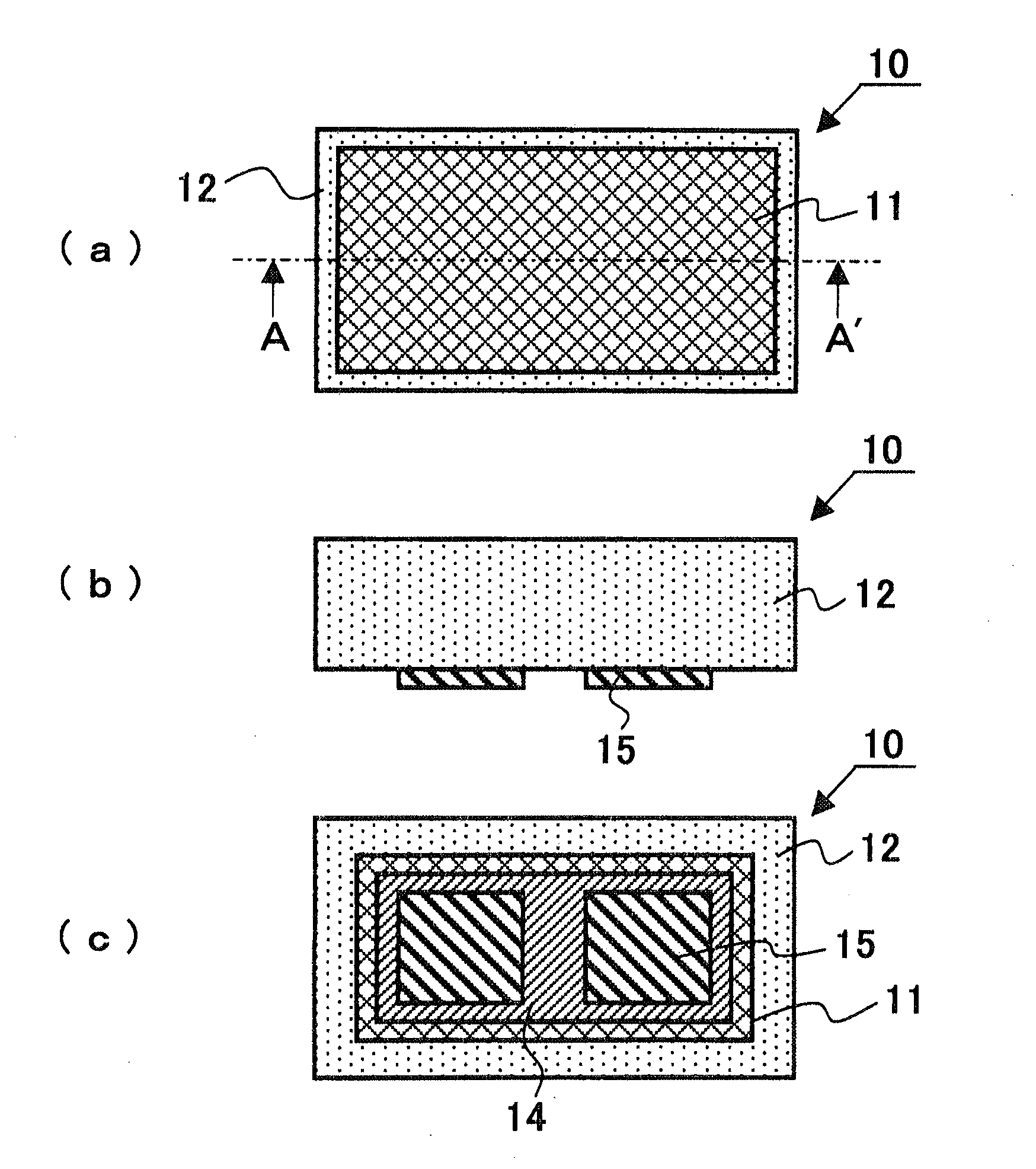
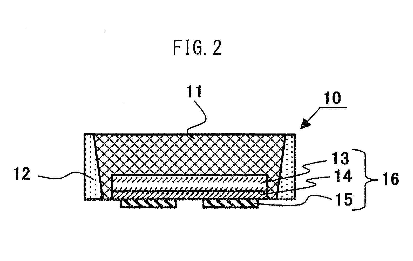
[0050]FIG. 1 shows the external appearance of an LED device 10; more specifically, FIG. 1(a) shows a plan view, FIG. 1(b) shows a front view, and FIG. 1(c) shows a bottom view.

[0051]As shown in FIG. 1(a), when the LED device 10 is viewed from the top, a rectangular reflective frame 12 and a phosphor member 11 enclosed th...


PUM


Abstract

Provided is an LED device which is compact while having good luminous efficiency and a focused light distribution. This LED device is provided with: a reflective frame around the outer periphery of the LED device; an LED die which has a transparent insulating substrate, a semiconductor layer formed on the bottom surface of the transparent insulating substrate, and an outer connection electrode disposed on the semiconductor layer; and a fluorescent member which is disposed on at least the top surface of the LED die and which converts the wavelength of the light emitted from the LED die. On the inside of the reflective frame is an inclined surface in contact with the lateral surface of the fluorescent member, and the inclined surface is formed such that the inner diameter of the reflective frame widens from the bottom surface towards the top surface of the LED die. Also provided is a manufacturing method of the LED device.

Description

CROSS REFERENCE TO RELATED APPLICATIONS[0001]This is the U.S. National Phase application of PCT / JP2013 / 081660, filed Nov. 25, 2013, which claims priority to Japanese Patent Application No. 2012-269210, filed Dec. 10, 2012, Japanese Patent Application No. 2013-003290, filed Jan. 11, 2013, the disclosures of these applications being incorporated herein by reference in their entireties for all purposes.TECHNICAL FIELD OF THE INVENTION[0002]The present invention relates to an LED device that lends itself to chip size packaging, and a method for manufacturing the same.BACKGROUND OF THE INVENTION[0003]With an increasing demand for higher brightness, the size of LED dies as bare chips has also been increasing, and nowadays, LED dies measuring up to 1 mm by 0.5 to 1 mm in area size are commercially available. Since this area size is about the same as that of other chip components such as resistors, there has developed a need for an LED device constructed by packaging an LED die with a resin...

Claims


Application Information

Patent Timeline
IPC IPC(8): H01L33/50H01L33/60H01L33/36
CPCH01L33/50H01L33/36H01L2933/0058H01L2933/0033H01L2933/0041H01L33/60H01L33/486H01L2224/13
Inventor OYAMADA, NODOKAIMAZU, KENJIMOCHIZUKI, SHUSAKU
Owner CITIZEN WATCH CO LTD
Why Eureka
Try Eureka