
Nanoparticle phosphor and method for manufacturing the same, semiconductor nanoparticle phosphor and light emitting element containing semiconductor nanoparticle phosphor, wavelength converter and light emitting device

a technology of nanoparticles and nanoparticles, which is applied in the direction of semiconductor devices, luminescent compositions, chemistry apparatuses and processes, etc., can solve the problems of affecting the light emission intensity of a phosphor, degrading the light emission efficiency of the phosphor containing the semiconductor nanoparticle, and non-radiative relaxation of exciton

Inactive Publication Date: 2015-11-05
SHARP KK
View PDF10 Cites 6 Cited by
  • Summary
  • Abstract
  • Description
  • Claims
  • Application Information

AI Technical Summary

Benefits of technology

The present invention provides a semiconductor nanoparticle phosphor with high light emission efficiency. The phosphor has a surface region with composition having high quantum confinement effect and containing two or more kinds of bonds. This surface region prevents non-radiative relaxation of excitons and deterioration of light emission property. The phosphor also has a modifying group that is not easily removed from the surface, which further enhances its light emission property. The method for manufacturing the phosphor includes steps of preparing a nanoparticle, surface-treating the nanoparticle, and supplying a raw material of a hetero atom to the nanoparticle.

Problems solved by technology

However, when the crystallinity of the nanoparticle or the surface state of the nanoparticle is not good, an exciton may undergo non-radiative relaxation (inactivation).
The energy level becomes a phenomenon of inhibiting the nature of the semiconductor nanoparticle having a narrow full width at half maximum, and it has been considered to be a problem to be solved.
For this reason, when the surface of the semiconductor nanoparticle undergoes influence of oxidation or the like, the chemical stability of the whole semiconductor nanoparticle is damaged, which greatly influences the light emission intensity of a phosphor.
For this reason, there is a problem that the light emission efficiency of the phosphor containing the semiconductor nanoparticle is degraded.

Method used


Image

  • Nanoparticle phosphor and method for manufacturing the same, semiconductor nanoparticle phosphor and light emitting element containing semiconductor nanoparticle phosphor, wavelength converter and light emitting device
  • Nanoparticle phosphor and method for manufacturing the same, semiconductor nanoparticle phosphor and light emitting element containing semiconductor nanoparticle phosphor, wavelength converter and light emitting device
  • Nanoparticle phosphor and method for manufacturing the same, semiconductor nanoparticle phosphor and light emitting element containing semiconductor nanoparticle phosphor, wavelength converter and light emitting device

Examples


first embodiment

Constitution of Nanoparticle Phosphor

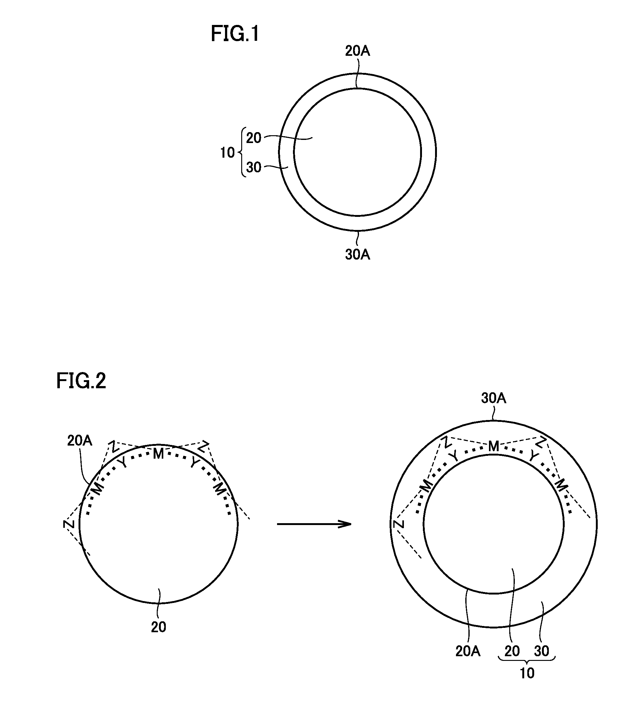
[0068]FIG. 1 is a cross-sectional view of a nanoparticle phosphor in a first embodiment of the present invention. A nanoparticle phosphor 10 includes a nanoparticle 20 and an inorganic substance layer 30. Nanoparticle 20 is composed of a compound semiconductor containing a first metal atom. Inorganic substance layer 30 is provided on the surface 20A of nanoparticle 20, and contains the first metal and one or more kinds of hetero atoms. In inorganic substance layer 30, the first metal atom is bound to the one or more kinds of hetero atoms (FIG. 2 right side).

[0069]FIG. 2 is a cross-sectional view schematically showing a manufacturing process of nanoparticle phosphor 10. In FIG. 2, M represents a first metal atom, Y represents an atom different from the first metal atom among atoms contained in nanoparticle 20, and Z represents a hetero atom. When a raw material of hetero atom Z is supplied to surface 20A of nanoparticle 20, first metal atom M posi...

second embodiment

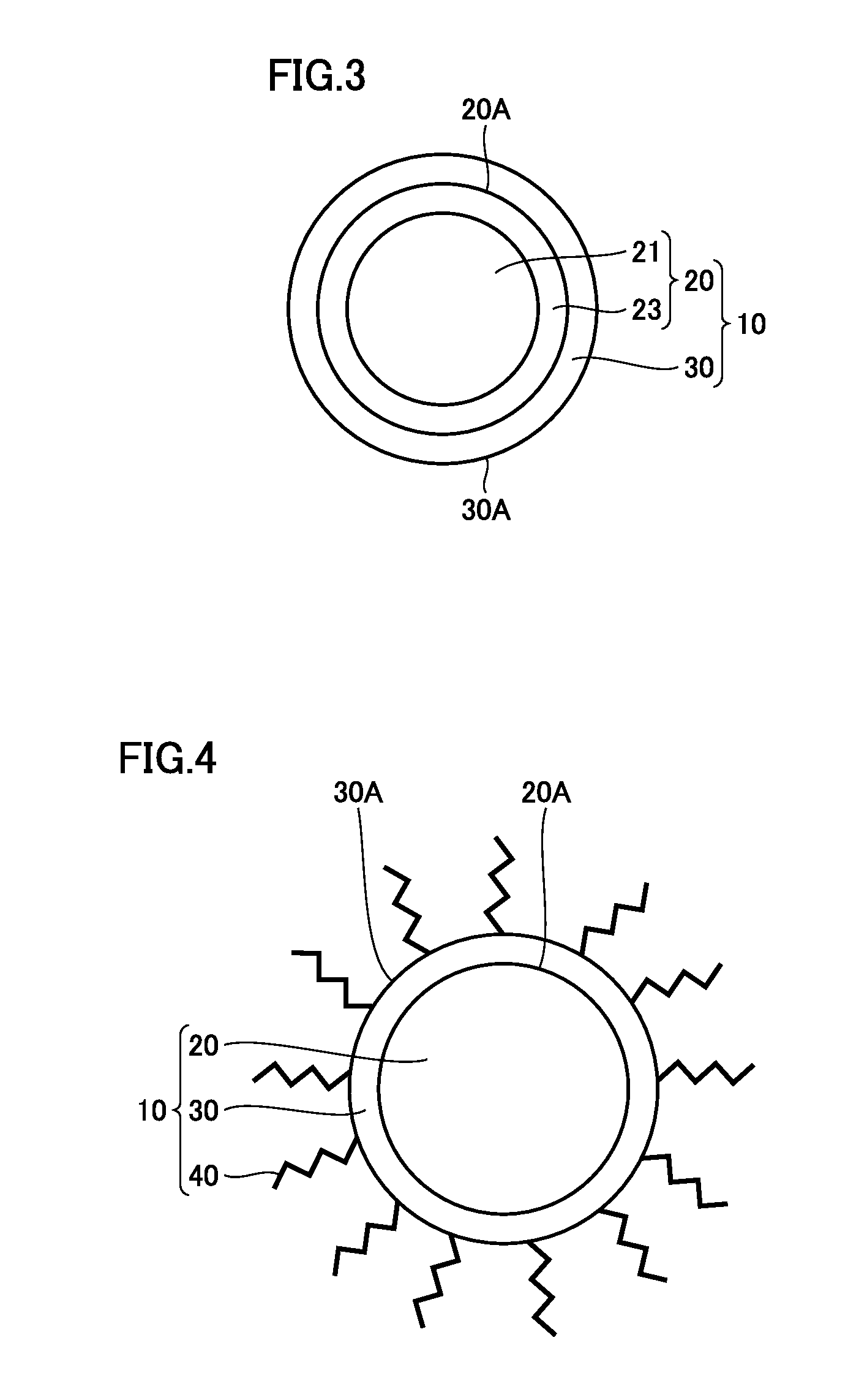
[0104]FIG. 3 is a cross-sectional view of a nanoparticle phosphor in a second embodiment of the present invention. In the present embodiment, nanoparticle 20 has a nanoparticle core 21 composed of a compound semiconductor, and a shell layer 23 covering nanoparticle core 21. Even in this case, the effect described in the first embodiment can be obtained. Not only this, but also nanoparticle phosphor 10 can have a wide range of utility. Points different from the first embodiment will be shown below.

[0105]

[0106]The compound semiconductor contained in nanoparticle core 21 is preferably any of the compound semiconductors described in the first embodiment. An average particle size of nanoparticle core 21 is preferably less than or equal to two times of the Bohr radius. The average particle size of nanoparticle core 21 can be estimated by directly observing a lattice image of nanoparticle core 21 with an observed image at high magnification, for example, using a scanning electron microscop...

third embodiment

[0113]FIG. 4 is a cross-sectional view of a nanoparticle phosphor in a third embodiment of the present invention. In the present embodiment, a modifying organic compound 40 is bound to the surface 30A of inorganic substance layer 30. Even in this case, the effect described in the first embodiment can be obtained. Not only this, but also the dispersibility of nanoparticle phosphor 10 can be enhanced, and therefore, the light emission property of nanoparticle phosphor 10 can be further enhanced. Points different from the first embodiment will be shown below.

[0114]

[0115]A chemical structure of modifying organic compound 40 is not particularly limited, but a length of modifying organic compound 40 in the radius direction of nanoparticle phosphor 10 is preferably greater than or equal to 0.1 nm and less than or equal to 5 nm. This makes it possible to prevent nanoparticle phosphors 10 from aggregation with each other, and therefore, the dispersibility of nanoparticle phosphor 10 can be e...


PUM


Abstract

A nanoparticle phosphor includes a nanoparticle composed of a compound semiconductor containing a first metal atom, and an inorganic substance layer provided on at least a part of the surface of the nanoparticle and containing the first metal atom and one or more kinds of hetero atoms. In the inorganic substance layer, the first metal atom is bound to the hetero atom.

Description

[0001]This nonprovisional application is based on Japanese Patent Application No. 2014-093538 filed on Apr. 30, 2014, No. 2014-240002 filed on Nov. 27, 2014, and No. 2014-245801 filed on Dec. 4, 2014, with the Japan Patent Office, the entire contents of which are hereby incorporated by reference.BACKGROUND OF THE INVENTION[0002]1. Field of the Invention[0003]The present invention relates to a nanoparticle phosphor and a method for manufacturing the same, a semiconductor nanoparticle phosphor and a light emitting element containing a semiconductor nanoparticle phosphor, a wavelength converter and a light emitting device.[0004]2. Description of the Background Art[0005]<First Background Art>[0006]It has been known that when an average particle size of crystal particles composed of a compound semiconductor is made to be approximately the Bohr radius, a quantum size effect is exhibited. The quantum size effect refers to the property of electrons in a substance, when made to be appr...

Claims


Application Information

Patent Timeline
IPC IPC(8): C09K11/70C09K11/62H01L33/50
CPCC09K11/703H01L33/502C09K11/623C09K11/62C09K11/621C09K11/701H01L33/44
Inventor MORISHITA, MAMIRYOHWA, TATSUYA
Owner SHARP KK
Learn More