Light-emitting device
a technology of light-emitting devices and light-emitting devices, which is applied in the direction of solid-state devices, semiconductor devices, thermoelectric devices, etc., to achieve the effect of reducing the variation in the amount of light emission of light-emitting devices
- Summary
- Abstract
- Description
- Claims
- Application Information
AI Technical Summary
Benefits of technology
Problems solved by technology
Method used
Image

Examples
example 1
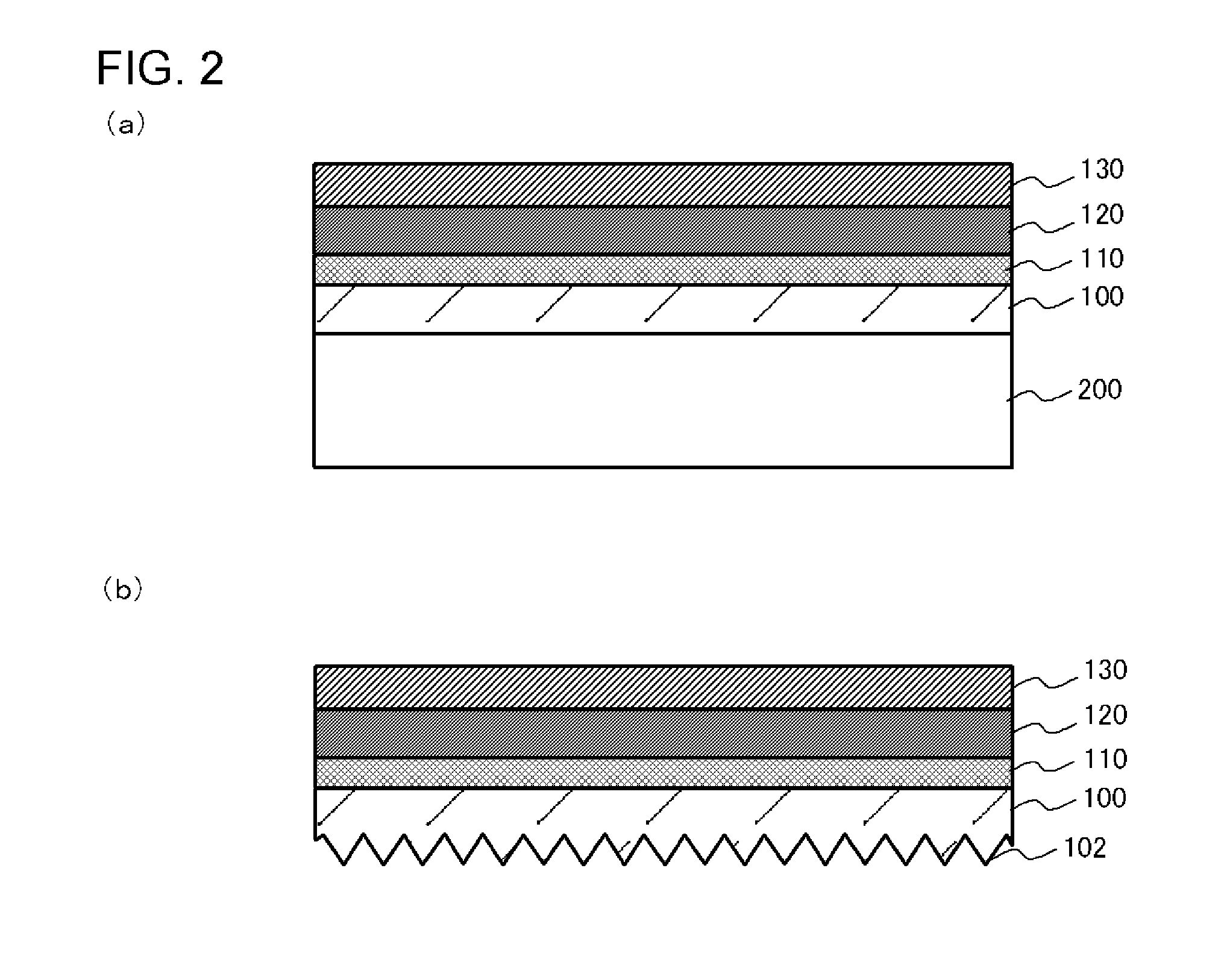
[0032]FIG. 3 is a cross-sectional view illustrating the configuration of a light-emitting device 10 according to Example 1. The light-emitting device 10 according to Example 1 has the same configuration as that of the light-emitting device 10 described in the embodiment except that a second light transmissive substrate 140 includes an irregularity formation layer 144.
[0033]The irregularity formation layer 144 is formed in a surface of the second light transmissive substrate 140 which faces the first light transmissive substrate 100. Second irregularities 142 are formed in the irregularity formation layer 144. For example, the irregularity formation layer 144 may be a film having the second irregularities 142, may be a layer obtained by firing glass paste, or may be a layer obtained by fixing inorganic particles (for example, SiO2 particles) to one surface of the second light transmissive substrate 140. When a film is used as the irregularity formation layer 144, a material of the fi...
example 2
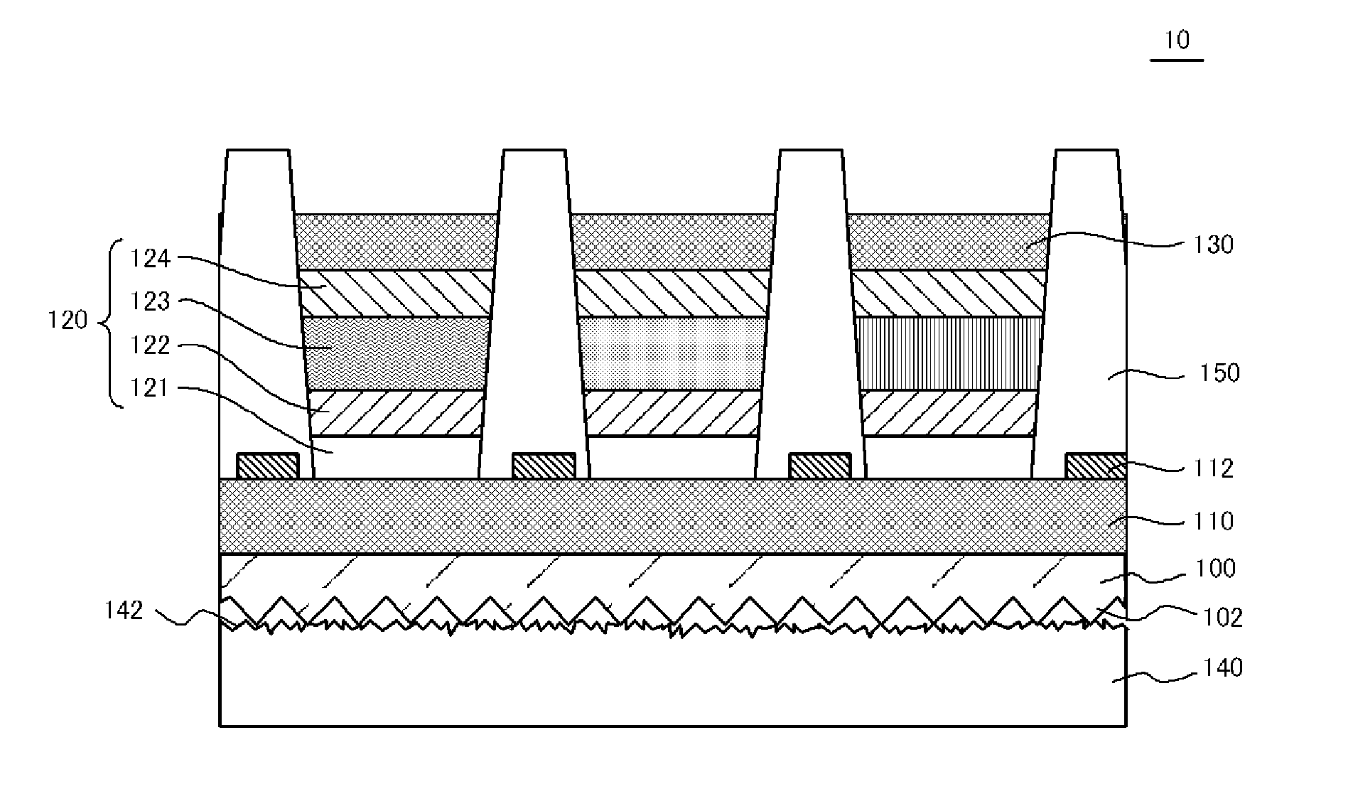
[0035]FIG. 4 is a cross-sectional view illustrating the configuration of a light-emitting device 10 according to Example 2. The light-emitting device 10 according to the present example has the same configuration as that of the light-emitting device 10 described in the embodiment except in the following respects.
[0036]First, an organic functional layer 120 is configured such that a hole injection layer 121, a hole transport layer 122, a light-emitting layer 123, and an electron injection layer 124 are laminated in this order.
[0037]In addition, the laminated structure of a first electrode 110, the hole injection layer 121, the hole transport layer 122, and the light-emitting layer 123 is divided into a plurality of regions. In detail, these laminated structures extend in parallel with each other in a direction perpendicular to the paper. The adjacent laminated structures are separated from each other by a partition wall 150. The partition wall 150 is a photosensitive resin such as, f...
example 3
[0043]FIG. 5 is a cross-sectional view illustrating the configuration of a light-emitting device 10 according to Example 3. The light-emitting device 10 according to the present example has the same configuration as that of the light-emitting device 10 according to Example 2 except that a first electrode 110 serves as a common electrode and an organic functional layer 120 serves as an electrode for each light-emitting region. In detail, an electron injection layer 124 and a second electrode 130 are individually provided in a plurality of light-emitting layers 123, and the first electrode 110 serves as a common electrode in the plurality of light-emitting layers 123.
[0044]Also in the present example, the same effects as in Example 2 can be obtained.
PUM
| Property | Measurement | Unit |
|---|---|---|
| depth | aaaaa | aaaaa |
| depth | aaaaa | aaaaa |
| depth | aaaaa | aaaaa |
Abstract
Description
Claims
Application Information
 - Generate Ideas
- Intellectual Property
- Life Sciences
- Materials
- Tech Scout
- Unparalleled Data Quality
- Higher Quality Content
- 60% Fewer Hallucinations
Browse by: Latest US Patents, China's latest patents, Technical Efficacy Thesaurus, Application Domain, Technology Topic, Popular Technical Reports.
© 2025 PatSnap. All rights reserved.Legal|Privacy policy|Modern Slavery Act Transparency Statement|Sitemap|About US| Contact US: help@patsnap.com