Delay line circuits and semiconductor integrated circuits

a technology of semiconductor integrated circuits and delay lines, which is applied in the direction of time-delay networks, multiple-port active networks, transistors, etc., can solve the problems of complex circuit layout of the internal module of the soc, inability to accurately achieve multiple relationships between, and waste of space, etc., to achieve uniform delay steps, shorten the design period, and reduce the effect of affecting

Active Publication Date: 2015-12-03
VIA ALLIANCE SEMICON CO LTD
View PDF2 Cites 0 Cited by
  • Summary
  • Abstract
  • Description
  • Claims
  • Application Information

AI Technical Summary

Benefits of technology

[0010]It is desirable to provide a delay line circuit which has a shorter design period, has uniform delay steps, and is less affected by the temperature and voltage, and which can be disposed in SOCs flexibly.

Problems solved by technology

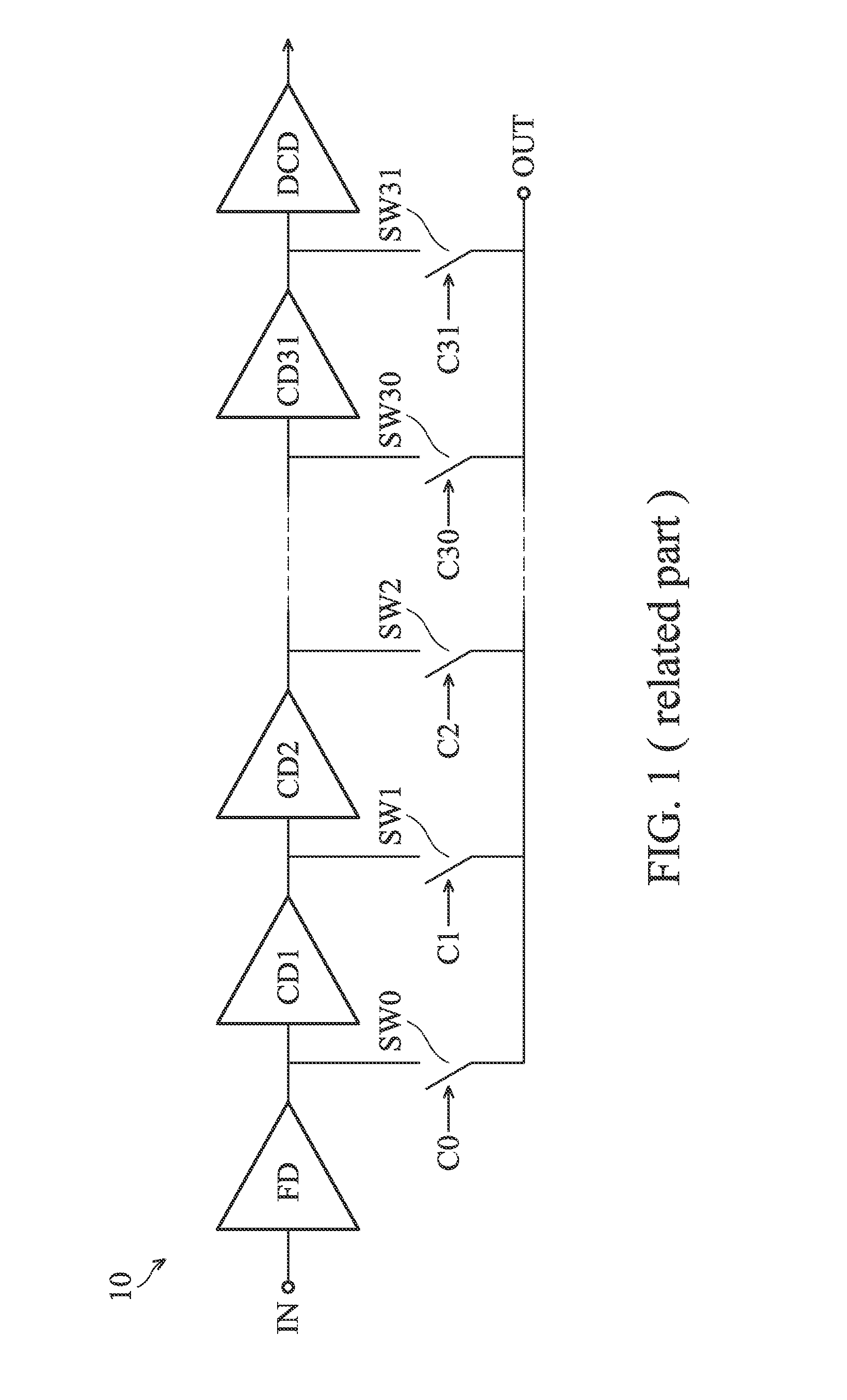
Since the delay of the fine delay unit FD and the delays of the coarse delay units CDN are generated in different ways, the multiple relationships therebetween cannot be achieved accurately, particularly when different power voltages and temperatures are involved.
Third. the fine delay unit FD and the coarse delay units CD1˜CD31 are arranged in a straight line in the circuit layout, however, this makes the circuit layouts of the internal module of the SOC complicated and wastes space, particularly, for 28 nm processes or advanced processes which require that polysilicons of all core transistors are arranged in the same direction.
In other words, different designs are required for different delay line circuits, which increases the cost.

Method used


Image

  • Delay line circuits and semiconductor integrated circuits
  • Delay line circuits and semiconductor integrated circuits
  • Delay line circuits and semiconductor integrated circuits

Examples


Embodiment Construction

[0027]This description is made for the purpose of illustrating the general principles of the invention and should not be taken in a limiting sense. In addition, the present disclosure may repeat reference numerals and / or letters in the various examples. This repetition is for the purpose of simplicity and clarity and does not in itself dictate a relationship between the various embodiments and / or configurations discussed. The scope of the invention is best determined by reference to the appended claims.

[0028]It is understood that the following disclosure provides many different embodiments, or examples, for implementing different features of the application. Specific examples of components and arrangements are described below to simplify the present disclosure. These are, of course, merely examples and are not intended to be limiting. In addition, the present disclosure may repeat reference numerals and / or letters in the various examples. This repetition is for the purpose of simpli...


PUM


Abstract

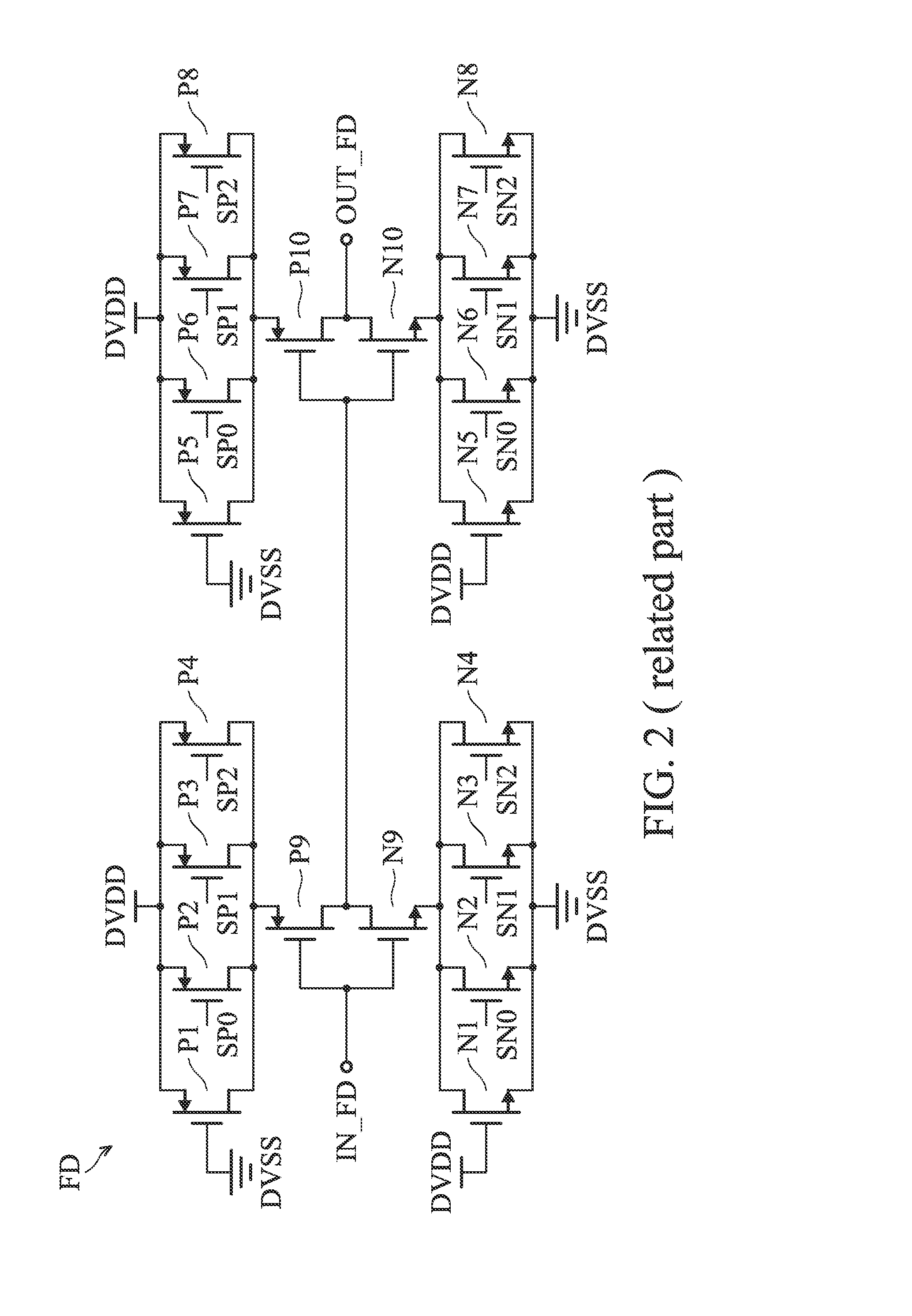
A delay line circuit is provided and includes a fine delay unit and coarse delay units. Each fine delay circuit includes a first PMOS transistor; a first NMOS transistor; second PMOS transistors whose widths of gate features of the second PMOS transistor are equal; at least one third PMOS transistor, coupled between the power voltage and the source of the first PMOS transistor, whose width of gate features is smaller than the widths of the gate features of the second PMOS transistors, second NMOS transistors whose widths of gate features of the second NMOS transistors are equal; and at least one third NMOS transistor, coupled between the ground voltage and the source of the first NMOS transistor, whose width of gate features is smaller than the widths of the gate features of the second NMOS transistors.

Description

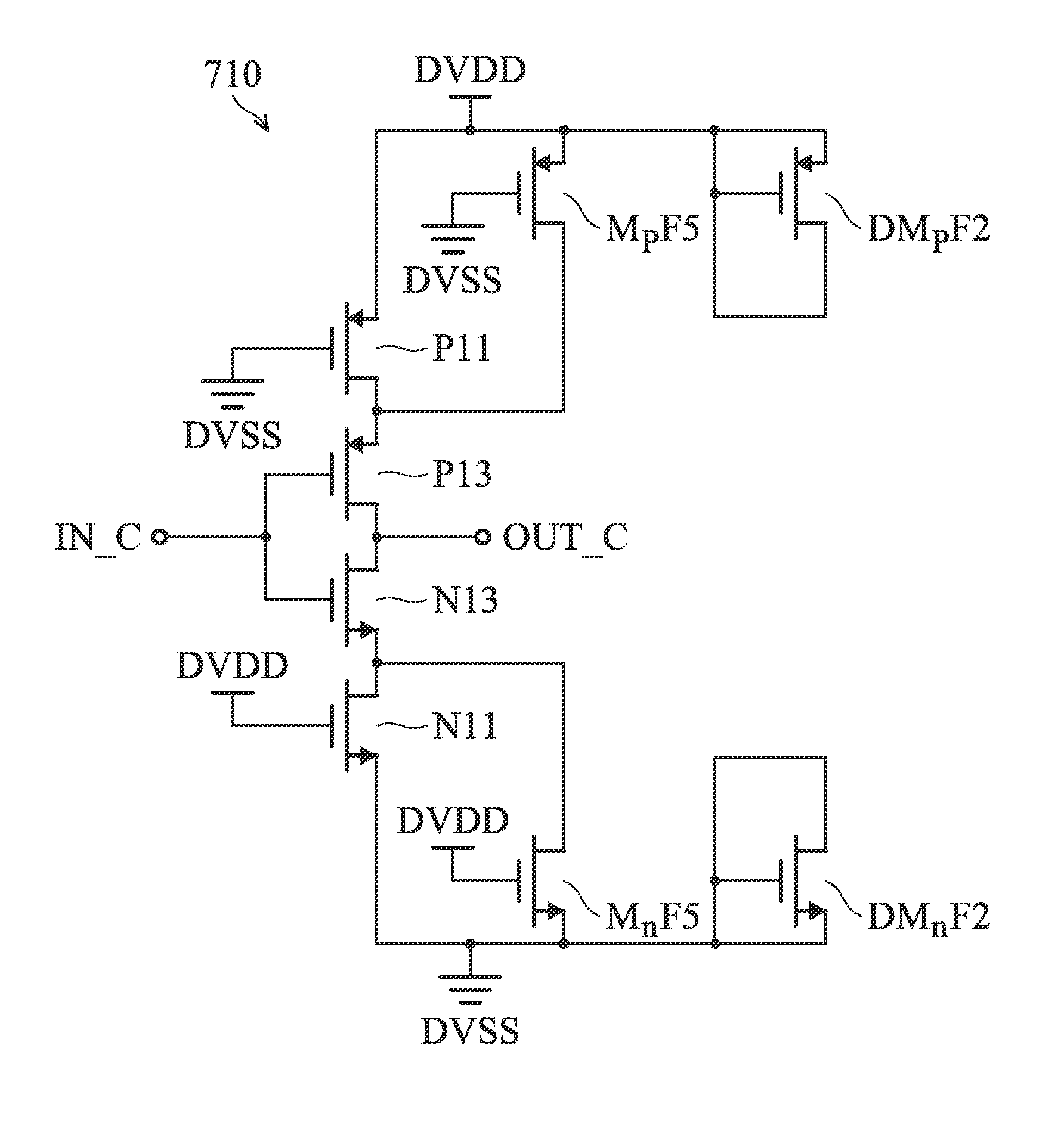
CROSS REFERENCE TO RELATED APPLICATIONS[0001]This Application claims priority of China Patent Application No. 201410235939.6, filed on May 29, 2014, the entirety of which is incorporated by reference herein.BACKGROUND OF THE INVENTION[0002]1. Field of the Invention[0003]The invention relates to a delay line circuit, and more particularly to a delay line circuit for a system-on-chip.[0004]2. Description of the Related Art[0005]In a system-one-chip, there are a large number of circuits which are used to process the phase relationship between signals. Multi-bit digital coding is required to control the phase relationship. A delay line circuit can be applied to achieve this function. For example, a delay line circuit can be controlled by 7-bit digital coding, so as to achieve delay adjustment by increasing 0˜127 delay steps for an input signal. Thus, the phase relationship between an output signal and a reference signal can be controlled.[0006]FIG. 1 shows a conventional delay line circ...

Claims


Application Information

Patent Timeline
Patent Type & Authority Applications(United States)
IPC IPC(8): H03K5/14
CPCH03K5/14H01L23/528H01L27/092
Inventor LIU, QUANFENGDUAN, HUIJIE
Owner VIA ALLIANCE SEMICON CO LTD
Why Eureka
Try Eureka