Active-matrix substrate, method of manufacturing active-matrix substrate, and display panel

a technology of active matrix and substrate, which is applied in the field of active matrix substrate, a method of manufacturing active matrix substrate, and a display panel, can solve the problems of restricting the design of the outer shape of the display, the difficulty of etc., and achieves the effect of improving the design freedom and reducing the size of the picture frame region

Active Publication Date: 2016-01-21
SHARP KK
View PDF6 Cites 118 Cited by
  • Summary
  • Abstract
  • Description
  • Claims
  • Application Information

AI Technical Summary

Benefits of technology

[0023]The present invention reduces the size of the picture-frame region of the active-matrix substrate and improves the freedom of design, such as the freedom in designing the active-matrix substrate.

Problems solved by technology

However, if gate drivers are disposed in the picture-frame region portion adjacent a side of the TFT substrate different from the side along which the source drivers are disposed on the TFT substrate as in JP 2012-103335 A, the lines and other components connecting the scan lines with the gate drivers must be routed along the picture-frame region of the TFT substrate, making it difficult to reduce the size of the picture-frame region, which means restrictions on the design of the outer shape of the display.

Method used


Image

  • Active-matrix substrate, method of manufacturing active-matrix substrate, and display panel
  • Active-matrix substrate, method of manufacturing active-matrix substrate, and display panel
  • Active-matrix substrate, method of manufacturing active-matrix substrate, and display panel

Examples


first embodiment

Construction of Liquid Crystal Display Device

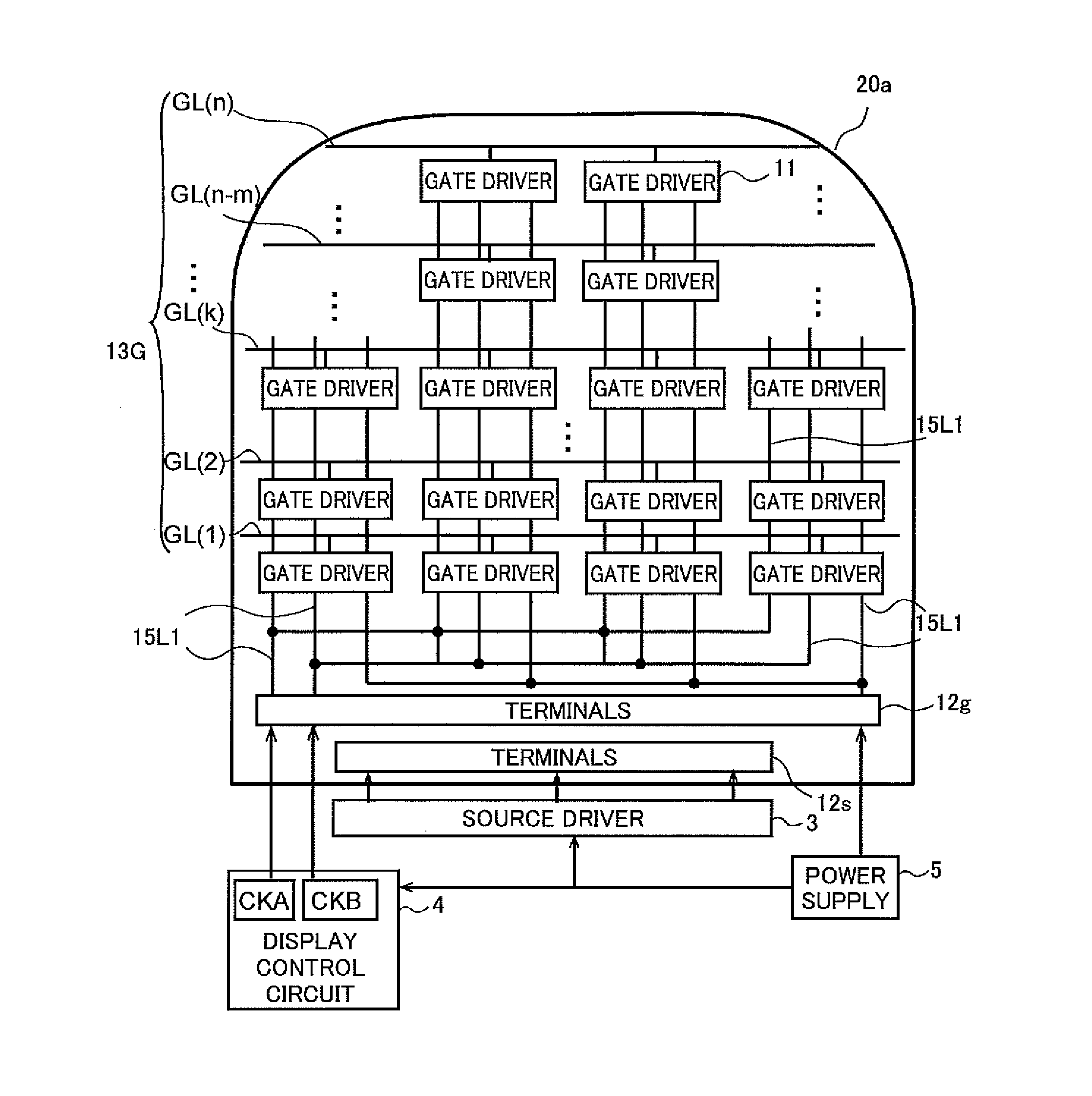
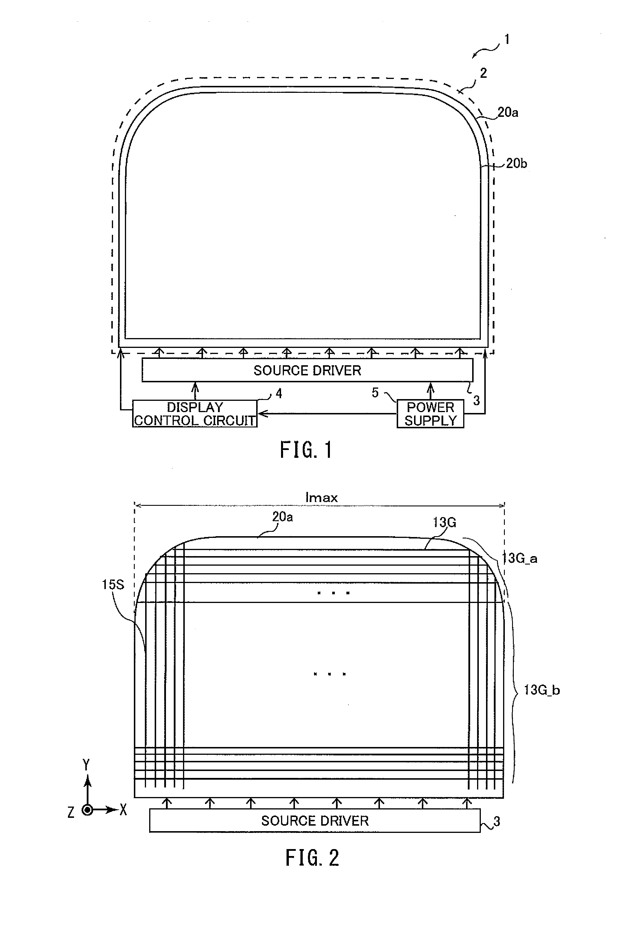
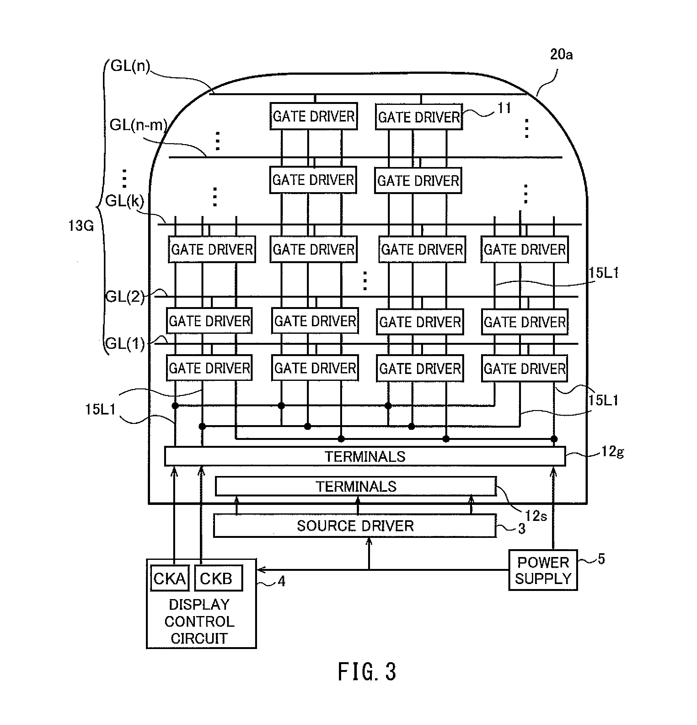
[0127]FIG. 1 is a schematic plan view of a liquid crystal display device according to the present embodiment. The liquid crystal display device 1 includes a display panel 2, a source device 3, a display control circuit 4, and a power supply 5. The display panel 2 includes an active-matrix substrate 20a, a counter-substrate 20b, and a liquid crystal layer (not shown) sandwiched between these substrates. Although not shown in FIG. 1, a polarizer is provided on the lower side of the active-matrix substrate 20a and another polarizer is provided on the upper side of the counter-substrate 20b. On the counter-substrate 20b are provided: a black matrix, red (R), green (G) and blue (B) color filters, and a common electrode (all not shown).

[0128]As shown in FIG. 1, the portion of the display panel 2 that is at the uppermost on paper, to the left and right, is arc-shaped. The active-matrix substrate 20a of the display panel 2 is electrically connect...

second embodiment

[0195]FIG. 10 is a schematic plan view of an active-matrix substrate according to the present embodiment. In this drawing, the same components as in the first embodiment are labeled with the same characters as in the first embodiment. The components that are different from those of the first embodiment will be described below. As shown in FIG. 10, the side of the active-matrix substrate 120a of the present embodiment that is parallel to the direction in which the gate lines 13G extend (i.e. X-direction) and is opposite to the side having the source driver 3 has protrusions and recesses. A group of gate lines 13G having a length that is substantially equal to the width of each recess / protrusion on the active-matrix substrate 120a as measured in the X-direction is provided in each of the columns having this width (hereinafter referred to as columns S1, S2, S3 and S4). That is, in the implementation of FIG. 10, each gate line 13G has a length that is smaller than the maximum value lmax...

third embodiment

[0202]The present embodiment describes an example active-matrix substrate having a non-display region within the display region. FIG. 12A is a schematic plan view of an active-matrix substrate according to the present embodiment. In FIG. 12A, the same components as in the first embodiment are labeled with the same characters as in the first embodiment. The components that are different from those of the first embodiment will be described below.

[0203]As shown in FIG. 12A, the active-matrix substrate 220a of the present embodiment includes a non-display region 300 within the display region 200 indicated by broken lines.

[0204]FIG. 12B is a cross-sectional view of the display panel 2 taken along line I-I of FIG. 12A. As shown in FIG. 12B, in the present embodiment, an element layer 10 including a gate line layer 13, source line layer 15 and semiconductor layer 14 is provided in the display region 200 on the substrate 20 of the active-matrix substrate 220a, and no element layer 10 is pre...


PUM


Abstract

An objective is to provide a technique for reducing the size of the picture-frame region of the active-matrix substrate and improve the freedom of design, such as the freedom in designing the active-matrix substrate. An active-matrix substrate includes a group of gate lines and a group of source lines crossing the gate lines. At least some of the gate lines have a length that is smaller than the maximum value of the width of the active-matrix substrate as measured in the direction in which the gate lines extend. The active-matrix substrate further includes pixel electrodes connected with the gate lines and source lines, and gate line driving units (11) provided in the display region for switching the gate lines to the selected or non-selected state in response to a supplied control signal. First terminals (12s) for providing data signals from the source driver and second terminals (12g) for providing control signals from the display control circuit are provided in the portion of the picture-frame region that is adjacent a side of the display region.

Description

TECHNICAL FIELD[0001]The present invention relates to an active-matrix substrate, a method of manufacturing an active-matrix substrate, and a display panel.BACKGROUND ART[0002]Display panels are known where gate drivers are provided along a side of an active-matrix substrate and source drivers are provided along an adjacent side thereof. JP 2012-103335 A discloses a display device having an atypically-shaped hexagonal display region provided by cutting off the corners of a rectangular one. Gate drivers and source drivers are disposed in the picture-frame region portions adjacent two adjacent sides of the TFT substrate of the display device. On the TFT substrate, a plurality of scan lines extend horizontally from the side thereof along which the gate drivers are provided, and a plurality of video signal lines extend vertically from the side thereof along which the source drivers are provided. The scan lines are connected with the gate drivers via lines provided along a portion of the...

Claims


Application Information

Patent Timeline
Patent Type & Authority Applications(United States)
IPC IPC(8): G09G3/36
CPCG09G3/3666G09G3/3677G09G2320/0233G09G2380/16G09G2300/0426G02F1/1345G09G3/20G09G2310/0218G09G3/3648G02F2201/56G09G2310/0278G09G2310/0281G09G2310/0291G02F1/13456
Inventor TANAKA, KOHHEIYOSHIDA, HIDEFUMI
Owner SHARP KK
Why Eureka
Try Eureka