Optical semiconductor device and method of producing the same

Active Publication Date: 2016-01-28
SUMITOMO ELECTRIC IND LTD
View PDF10 Cites 12 Cited by
  • Summary
  • Abstract
  • Description
  • Claims
  • Application Information

AI Technical Summary

Benefits of technology

[0007]In this optical semiconductor device, the resin layer is disposed on the principal surface of the substrate, top surfaces of the first and second signal electrodes, and the resistor. The capacitor is disposed on the resin layer. The resin layer covers the optical waveguide and the signal electrode. The resin layer has

Problems solved by technology

It is difficult to monolithically integrate a capacitor ha

Method used


Image

  • Optical semiconductor device and method of producing the same
  • Optical semiconductor device and method of producing the same
  • Optical semiconductor device and method of producing the same

Examples


Example

[0018]First, the details of an embodiment of the present invention will be listed and described.

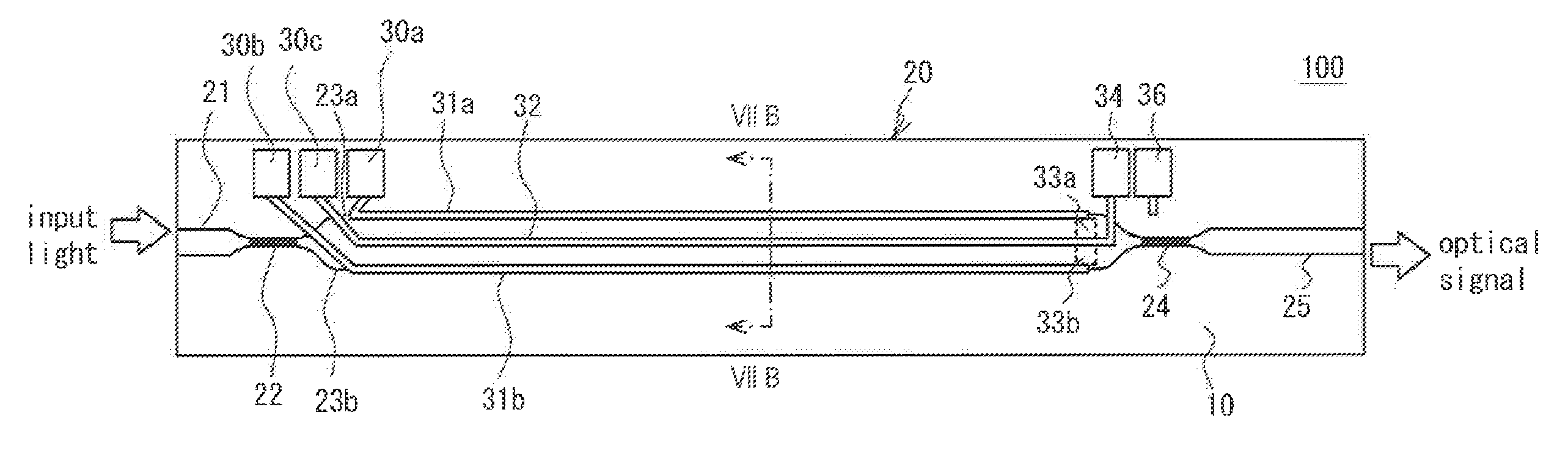
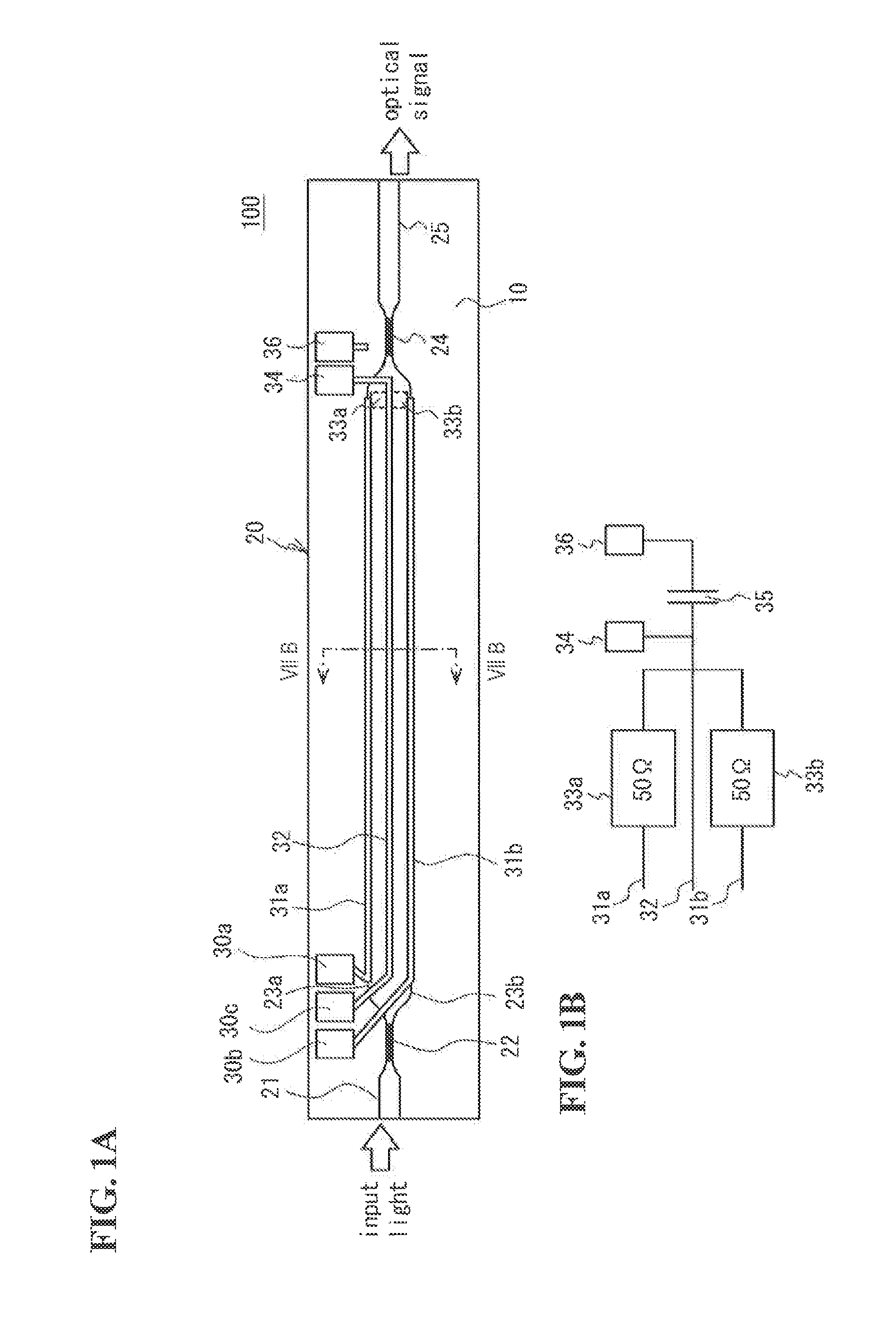
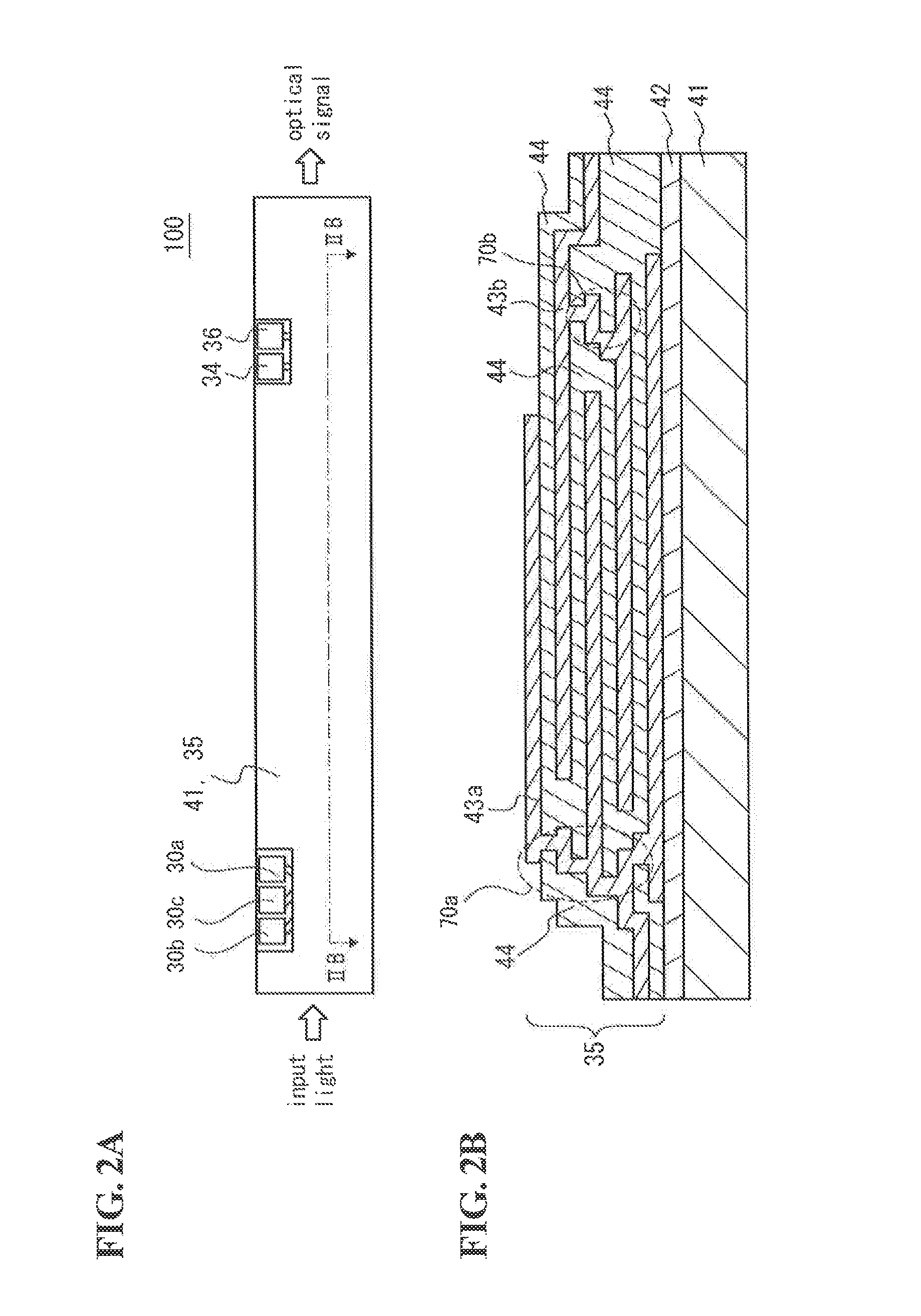
[0019]The present invention relates to an optical semiconductor device including a substrate having a principal surface and a back surface opposite to the principal surface; a first optical waveguide disposed on the principal surface of the substrate, the first optical waveguide extending in a first direction; a second optical waveguide disposed on the principal surface of the substrate, the second optical waveguide extending in the first direction, the second optical waveguide being arranged adjacent to the first optical waveguide in a second direction intersecting with the first direction; a first signal electrode disposed on the first optical waveguide; a second signal electrode disposed on the second optical waveguide; a resistor disposed on the principal surface of the substrate, the resistor being arranged between the first optical waveguide and the second optical waveguide, the res...


PUM


Abstract

An optical semiconductor device including: a substrate having a principal surface; a first and a second optical waveguides disposed on the principal surface of the substrate, the first and second optical waveguides extending in a first direction, the second optical waveguide being arranged adjacent to the first optical waveguide in a second direction intersecting with the first direction; a first and a second signal electrodes disposed on the first and second optical waveguides; a resistor disposed on the principal surface, the resistor being arranged between the first optical waveguide and the second optical waveguide, the resistor being electrically connected to the first signal electrode and the second signal electrode; a resin layer disposed on the principal surface, top surfaces of the first and second signal electrodes, and the resistor; and a capacitor disposed on the resin layer, the capacitor being electrically connected to the resistor through an opening of the resin layer.

Description

BACKGROUND OF THE INVENTION[0001]1. Field of the Invention[0002]The present invention relates to an optical semiconductor device and a method of producing the same,[0003]2. Description of the Related Art[0004]Japanese Unexamined Patent Application Publication No. 2007-180425 (Patent Literature 1) discloses a semiconductor device including a capacitor and an optical element monolithically integrated on a single substrate. The capacitor is used to eliminate noise components in electrical signals applied to the semiconductor device. Noise components are transmitted from the outside of the semiconductor device and reach the semiconductor device through an electrical line. If the elimination of the noise components by the capacitor is insufficient, a malfunction occurs in the optical element of the semiconductor device. In order to sufficiently eliminate noise components having high frequencies, a capacitor having a large capacitance is desired.SUMMARY OF THE INVENTION[0005]In the semico...

Claims


Application Information

Patent Timeline
IPC IPC(8): G02F1/225G02B6/132
CPCG02F1/2257G02F2001/212G02B6/132G02B6/136G02F1/025G02F1/2255G02F2201/12G02F1/212
Inventor MASUYAMA, RYUJIKONO, NAOYAKIMURA, DAISUKEKOBAYASHI, HIROHIKOKITAMURA, TAKAMITSUYAGI, HIDEKI
Owner SUMITOMO ELECTRIC IND LTD
Why Eureka
Try Eureka