

Semiconductor element and semiconductor device
a semiconductor and semiconductor technology, applied in the direction of semiconductor devices, semiconductor/solid-state device details, diodes, etc., can solve the problem of difficult to reduce the side of the diode , achieve the effect of maintaining the allowable electrical current at a high level and reducing the size of the diod
- Summary
- Abstract
- Description
- Claims
- Application Information
AI Technical Summary
Benefits of technology
Problems solved by technology
Method used
Image

Examples
first embodiment
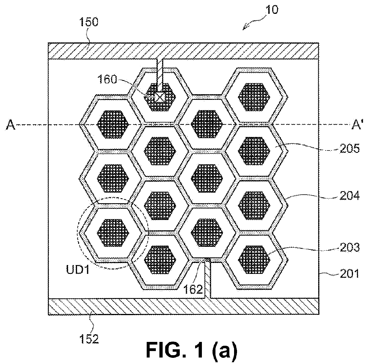
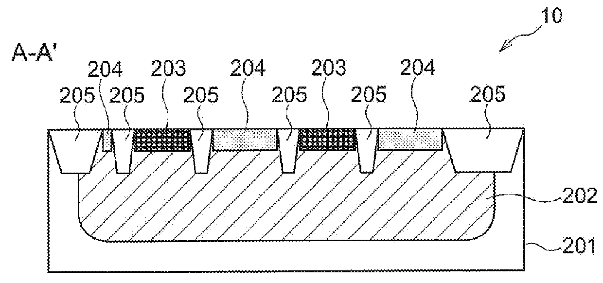
[0031]A first embodiment of the present invention will be explained. FIGS. 1(a) and 1(b) are schematic views showing a configuration of a diode 10 as a semiconductor element according to the first embodiment of the present invention. More specifically, FIG. 1(a) is a schematic plan view showing the diode 10 as the semiconductor element, and FIG. 1(b) is a schematic sectional view showing the diode 10 as the semiconductor element taken along a line A-A′ in FIG. 1(a).
[0032]As shown in FIG. 1(a), the diode 10 includes a P-type substrate 201; a plurality of P-type high concentration diffusion layers 203 formed in the substrate; and an N-type high concentration diffusion layer 204 formed in the substrate. Each of the P-type high concentration diffusion layers 203 and a part of the N-type high concentration diffusion layer 204 surrounding each of the P-type high concentration diffusion layers 203 constitute a unit element UD1 arranged adjacent to each other at a plurality of locations (fo...
second embodiment
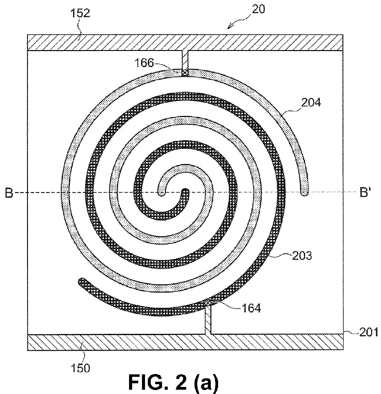
[0052]A second embodiment of the present invention will be explained with reference to FIGS. 2(a) and 2(b). FIGS. 2(a) and 2(b) are schematic views showing a configuration of a diode 20 as a semiconductor element according to a second embodiment of the present invention. More specifically, FIG. 2(a) is a schematic plan view showing the diode 20 as the semiconductor element, and FIG. 2(b) is a schematic sectional view showing the diode 20 as the semiconductor element taken along a line B-B′ in FIG. 2(a).
[0053]In the second embodiment, the diode 20 includes the P-type high concentration diffusion layer 203 and the N-type high concentration diffusion layer 204 having shapes different from those of the P-type high concentration diffusion layer 203 and the N-type high concentration diffusion layer 204 of the diode 10 in the first embodiment. Components in the second embodiment similar to those in the first embodiment are designated with the same reference numerals, and explanations there...
PUM
 Abstract
Description
Claims
Application Information