Method and apparatus for calibrating CMOS inverter
Active Publication Date: 2016-02-04
REALTEK SEMICON CORP
View PDF1 Cites 9 Cited by
Summary
Abstract
Description
Claims
Application Information
AI Technical Summary
This helps you quickly interpret patents by identifying the three key elements:
Problems solved by technology
Method used
Benefits of technology
[0008]An objective of this present invention is to calibrate a tunable CMOS inverter so that two of such tunable CMOS inverte
Problems solved by technology
The calibration scheme taught by Zeller et al, neglects the effect of the output re
Method used
Image
Click on the blue label to locate the original text in one second.
Reading with bidirectional positioning of images and text.
Examples
Embodiment Construction
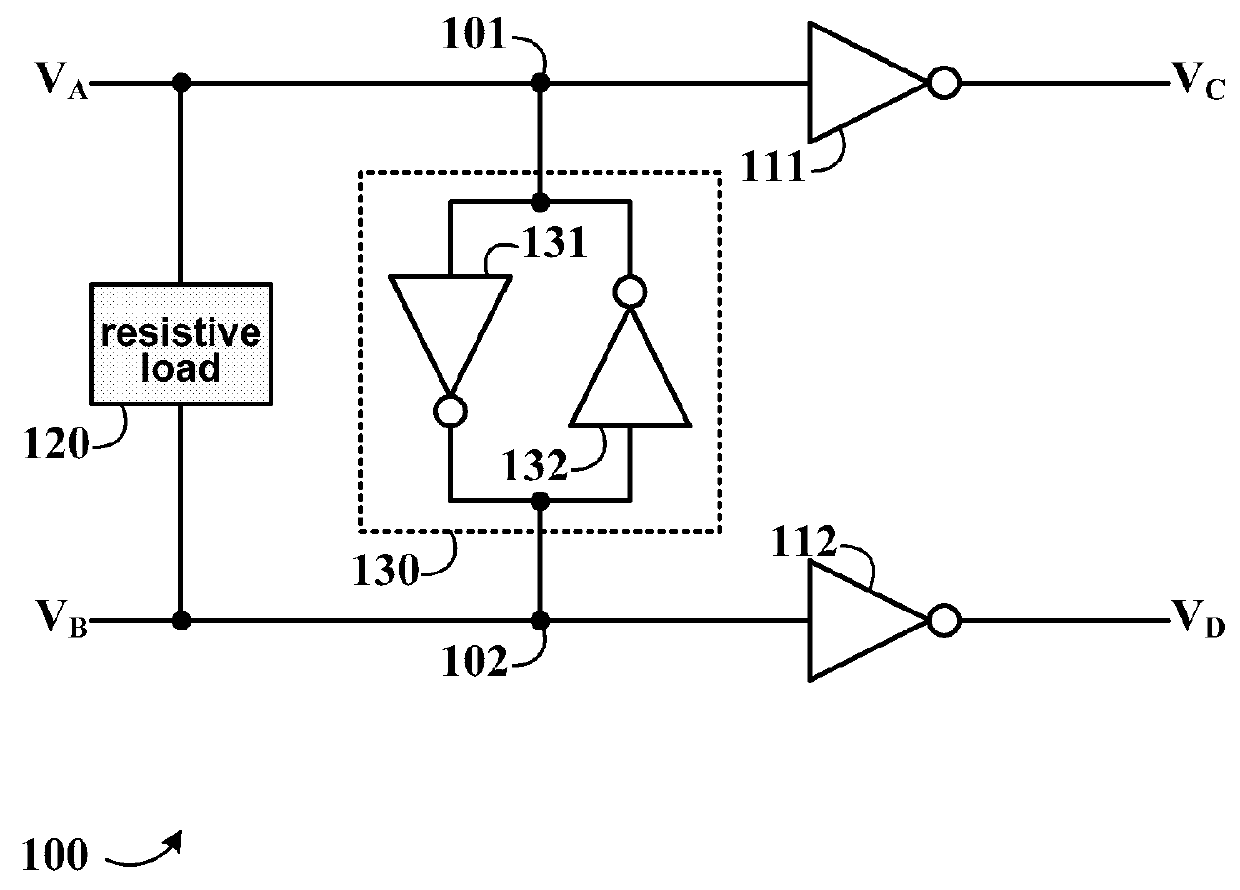
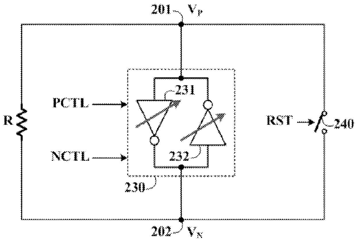
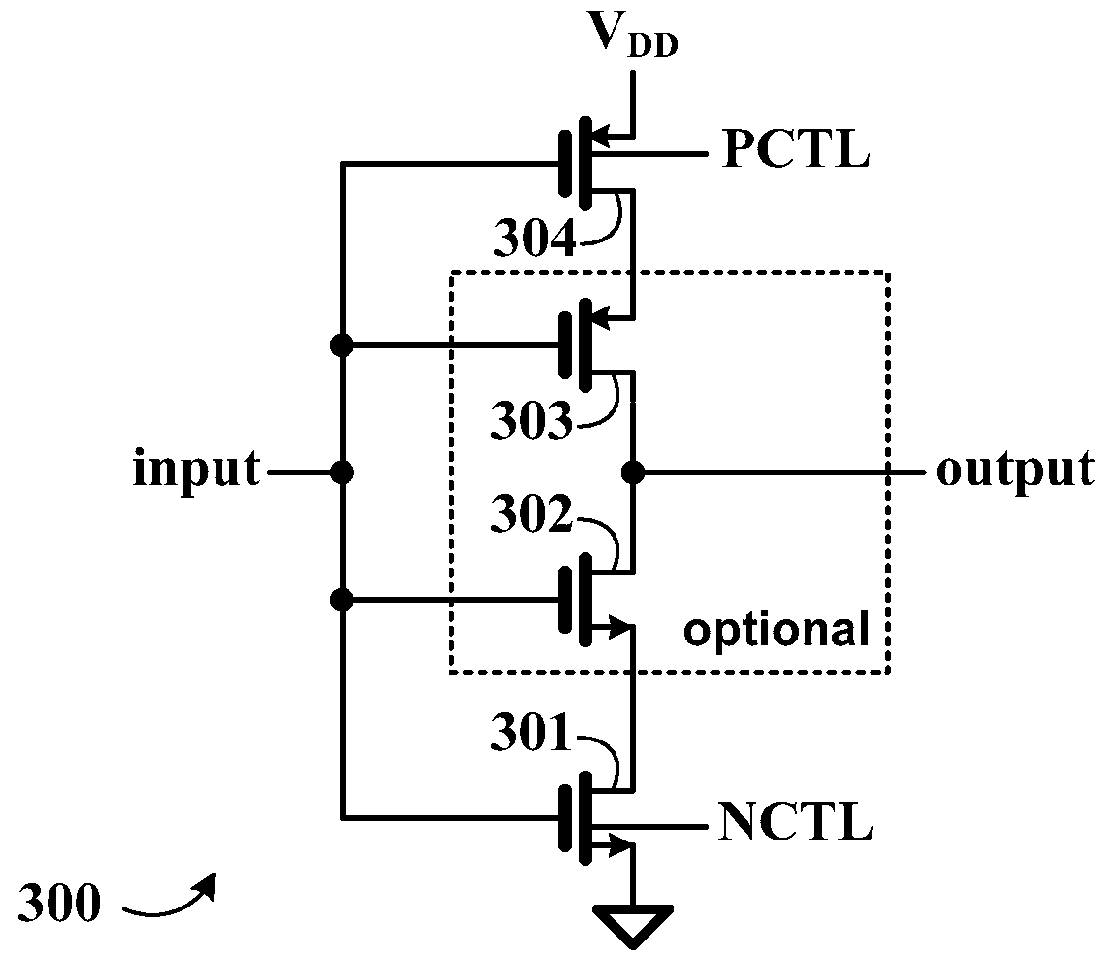
[0017]The present invention relates to CMOS inverter. While the specification describes several example embodiments of the invention considered favorable modes of practicing the invention, it should be understood that the invention can be implemented in many ways and is not limited to the particular examples described below or to the particular manner in which any features of such examples are implemented. In other instances, well-known details are not shown or described to avoid obscuring aspects of the invention.
[0018]Throughout this disclosure: “VDD” denotes a power supply node of a power supply (voltage) level; a ground symbol denotes a ground node of a ground (voltage) level; a CMOS inverter comprises a PMOS transistor, of which a source terminal is connected to the power supply node, a gate terminal is connected to an input of the CMOS inverter, and a drain terminal is coupled to an output of the CMOS inverter, and a NMOS transistor, of which a source terminal is connected to ...
PUM
Abstract
A circuit and method for calibrating CMOS (complementary metal-oxide semiconductor) inverters are provided. In a circuit, a first tunable CMOS inverter, controlled by a control signal, receives a first voltage from a first circuit node and outputs a second voltage to a second circuit node. A second tunable CMOS inverter, controlled by the control signal, receives the second voltage from the second circuit node and outputs the first voltage to the first circuit node. A resistor couples the first circuit node to the second circuit node. A switch, controlled by a reset signal, conditionally shorts the first circuit node to the second circuit node. A finite state machine receives the first voltage and the second voltage and outputs the reset signal and the control signal, wherein the control signal is adjusted based on a difference between the first voltage and the second voltage.
Description
BACKGROUND OF THE INVENTION[0001]1. Field of the Invention[0002]The present invention generally relates to CMOS (complimentary metal oxide semiconductor) inverter circuits and more particularly to a method and apparatus for calibrating CMOS inverter circuits.[0003]2. Description of Related Art[0004]Persons of ordinary skill in the art understand terms and basic concepts related to microelectronics that are used in this disclosure, such as MOS (metal-oxide semiconductor) transistor, PMOS (p-channel MOS) transistor, NMOS (n-channel MOS) transistor, CMOS, “operational amplifier,”“common-mode,”“differential-mode”“transconductance,”“output resistance”“gate,”“source,”“drain,”“saturation region,”“trip point,”“bulk,”“cascode,”“switch,”“voltage,”“current,”“circuit,”“circuit node,”“power supply,”“ground,”“rail,”“latch,”“negative resistance,” and “inverter”. Terms and basic concepts like these are apparent from prior art documents, e.g. text books such as “Design of Analog CMOS Integrated Circ...
Claims
Application Information
Patent Timeline
Application Date:The date an application was filed.
Publication Date:The date a patent or application was officially published.
First Publication Date:The earliest publication date of a patent with the same application number.
Issue Date:Publication date of the patent grant document.
PCT Entry Date:The Entry date of PCT National Phase.
Estimated Expiry Date:The statutory expiry date of a patent right according to the Patent Law, and it is the longest term of protection that the patent right can achieve without the termination of the patent right due to other reasons(Term extension factor has been taken into account ).
Invalid Date:Actual expiry date is based on effective date or publication date of legal transaction data of invalid patent.