Light-emitting device and image forming apparatus

a technology of light-emitting devices and image forming apparatuses, which is applied in the direction of recording devices, static indicating devices, instruments, etc., can solve the problems of difficulty in accurately controlling the amount of current flowing into each organic el element, and achieve accurate control of the amount of current flow, fine image formation, and reduced waveform deformation

Active Publication Date: 2016-02-11
CANON KK
View PDF2 Cites 3 Cited by
  • Summary
  • Abstract
  • Description
  • Claims
  • Application Information

AI Technical Summary

Benefits of technology

[0009]An object of the present invention is to provide a light-emitting device accurately controlling the amount of current to be flowed to each light-emitting element by reducing the deformation of the waveforms of control signals, and also to provide an image forming apparatus with such a light-emitting device capable of fine image formation.

Problems solved by technology

Such a difference influences the writing of a data signal to each pixel circuit and makes it difficult to accurately control the amount of current to be flowed into each organic EL element.

Method used


Image

  • Light-emitting device and image forming apparatus
  • Light-emitting device and image forming apparatus
  • Light-emitting device and image forming apparatus

Examples


first embodiment

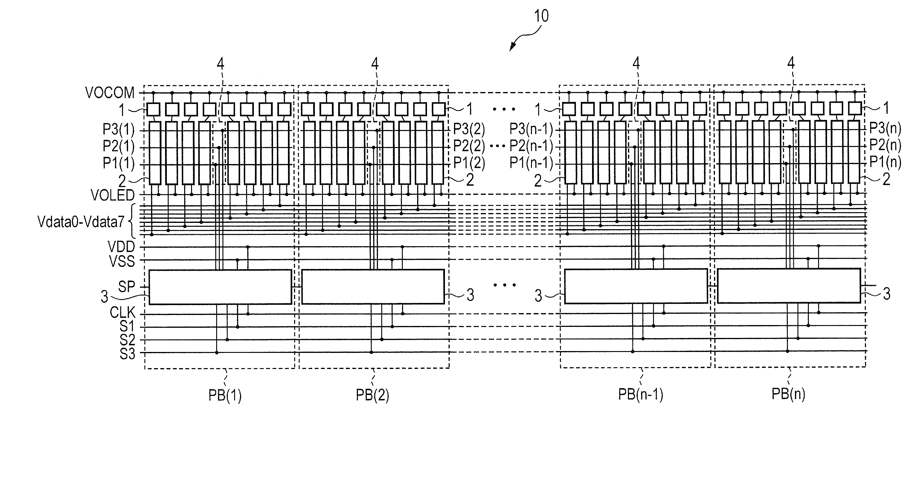
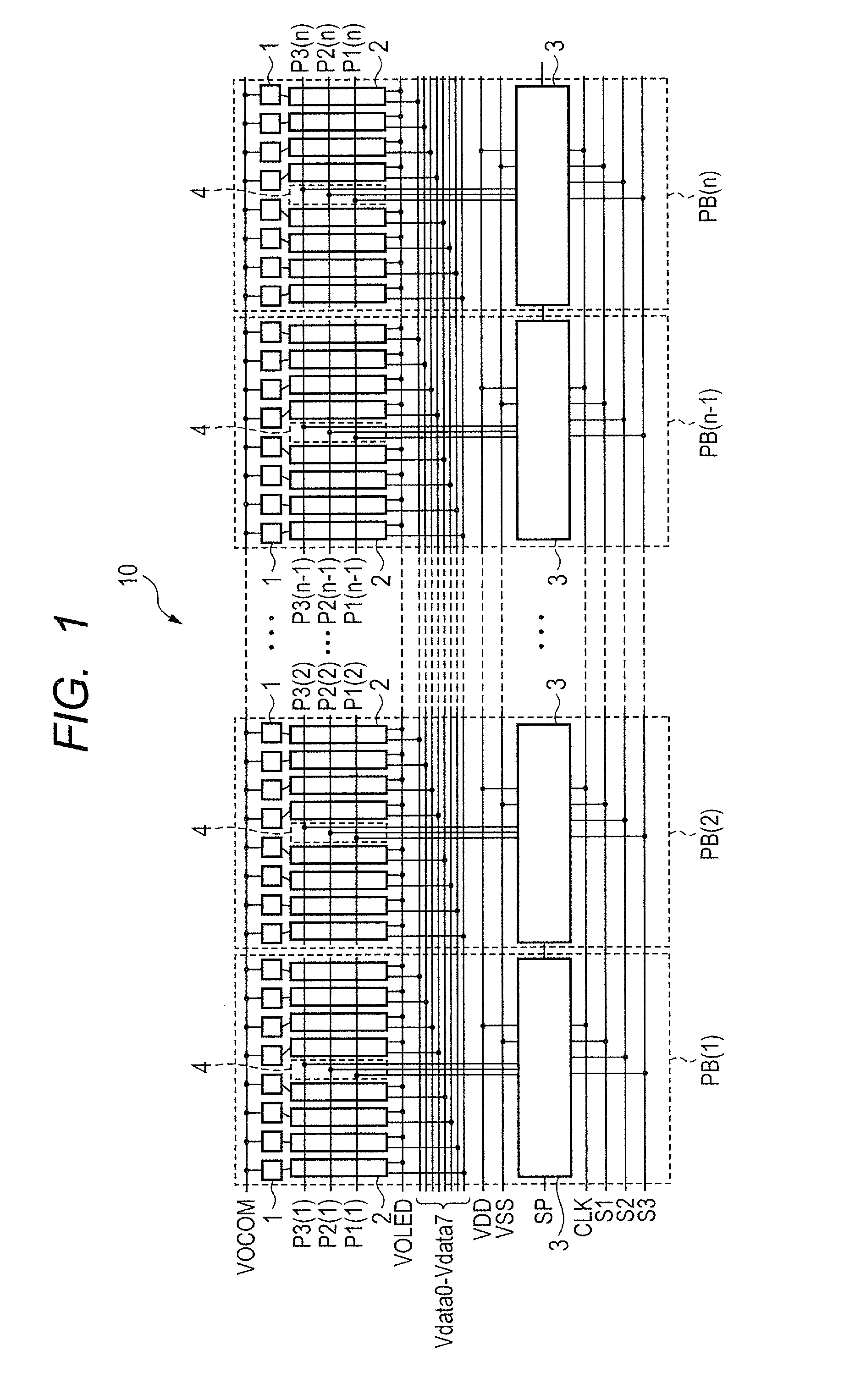
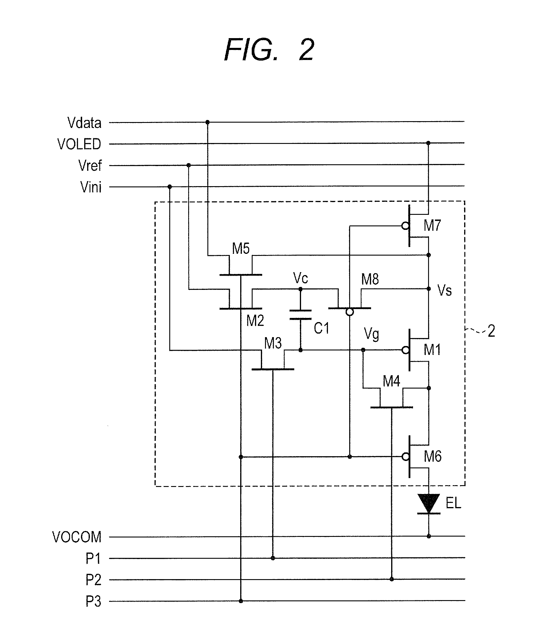
[0019]A light-emitting device according to a first embodiment of the present invention will be described with reference to FIGS. 1 to 3. FIG. 1 is a schematic diagram illustrating the configuration of the light-emitting device according to the present embodiment. FIG. 2 is a circuit diagram illustrating an example of a pixel circuit in the light-emitting device according to the present embodiment. FIG. 3 is a timing chart illustrating the operation of the light-emitting device according to the present embodiment.

[0020]First, the configuration of the light-emitting device according to the present embodiment will be described with reference to FIGS. 1 and 2.

[0021]The light-emitting device according to the present embodiment is applicable as, but not particularly limited to, for example, an exposure head in an image forming apparatus such as a laser printer, etc. for irradiating a photosensitive drum with light to form a latent image thereon.

[0022]As illustrated in FIG. 1, a light-emit...

second embodiment

[0067]A light-emitting device according to a second embodiment of the present invention will be described with reference to FIG. 4. FIG. 4 is a schematic diagram illustrating the configuration of the light-emitting device according to the present embodiment. Constituent components similar to those of the light-emitting device according to the first embodiment, which are illustrated in FIGS. 1 to 3, will be denoted by the same reference signs, and will not be described or will be described briefly.

[0068]In the present embodiment, only the difference from the light-emitting device according to the first embodiment, which is illustrated in FIG. 1, will be described. Note that FIG. 4 only illustrates a pixel block PB(1) and a pixel block PB(2) among n pixel blocks PB for the sake of simplicity.

[0069]In the light-emitting device according to the first embodiment, the plurality of pixel circuits 2 included in each pixel block PB are divided into two groups each including a half of the pix...

third embodiment

[0072]A light-emitting device according to a third embodiment of the present invention will be described with reference to FIG. 5. FIG. 5 is a schematic diagram illustrating the configuration of the light-emitting device according to the present embodiment. Constituent components similar to those of the light-emitting devices according to the first and second embodiments, which are illustrated in FIGS. 1 to 4, will be denoted by the same reference signs, and will not be described or will be described briefly.

[0073]In the present embodiment, only the difference from the light-emitting devices according to the first and second embodiments, which are illustrated in FIGS. 1 and 4, will be described. Note that FIG. 5 only illustrates a pixel block PB(1) and a pixel block PB(2) among n pixel blocks PB for the sake of simplicity.

[0074]In the first and second embodiments, the plurality of pixel circuits 2 included in each pixel block PB are divided into two groups. However, the pixel circui...


PUM


Abstract

The present invention provides a light-emitting device including a pixel block including light-emitting elements disposed on a long substrate and aligned in the longitudinal direction of the substrate, pixel circuits connected to the light-emitting elements, a control signal line connected to the pixel circuits, and a pixel block select circuit connected to the control signal line and configured to output a control signal to the pixel circuits. The pixel circuits are divided into a plurality of groups. The control signal line includes first and second interconnection portions. The first interconnection portion is disposed along the longitudinal direction of the substrate and connected to the pixel circuits. The second interconnection portion is disposed in a region between the groups and connected to the pixel block select circuit. The first interconnection portion and the second interconnection portion are connected to each other in the region between the groups.

Description

BACKGROUND OF THE INVENTION[0001]1. Field of the Invention[0002]The present invention relates to a light-emitting device and an image forming apparatus.[0003]2. Description of the Related Art[0004]In recent years, image forming apparatuses have been developed which use, as exposure means, a line head with many organic electroluminescence elements (hereinafter, referred to as “organic EL elements”) disposed in one line. This line head includes the plurality of organic EL elements and a plurality of pixel circuits including transistors for driving these organic EL elements. The luminance of each organic EL element is controlled by controlling the amount of current to be flowed into the organic EL element by means of the corresponding pixel circuit.[0005]Japanese Patent Application Laid-Open No. 2009-006718 discloses a line head using organic EL elements disposed in a line. The line head described in Japanese Patent Application Laid-Open No. 2009-006718 is such that a plurality of pixe...

Claims


Application Information

Patent Timeline
Patent Type & Authority Applications(United States)
IPC IPC(8): H05B41/36B41J2/385H05B44/00
CPCG09G3/3233G09G3/3225H05B33/0896G03G15/04054G09G2310/0256G09G2300/0819G09G2320/043G09G2300/0866G09G2310/0251G09G2300/0861G09G2310/0262G09G2320/0223
Inventor GODEN, TATSUHITOSAKAGUCHI, KIYOFUMI
Owner CANON KK
Why Eureka
Try Eureka