Process for manufacturing a composite structure

Active Publication Date: 2016-02-11
SOITEC
View PDF10 Cites 1 Cited by
  • Summary
  • Abstract
  • Description
  • Claims
  • Application Information

AI Technical Summary

Benefits of technology

[0069]Thus, a simple step is observed and the peripheral portion corresponds to a stack comprising a single intermediate layer.
[0070]Consequently, the composite

Problems solved by technology

The main drawback of this manufacturing method is, therefore, t

Method used


Image

  • Process for manufacturing a composite structure
  • Process for manufacturing a composite structure
  • Process for manufacturing a composite structure

Examples


Example

First Embodiment

[0138]The first embodiment is illustrated in FIGS. 4A and 4B.

[0139]Formation of the Dielectric Layer 30

[0140]The dielectric layer 30 may be formed in two steps:[0141]b1) formation of a layer of dielectric material of the donor substrate 10;[0142]b2) partial removal of the layer of dielectric material so that the residual layer of dielectric material forms the dielectric layer 20.

[0143]Step b1) may be a technique of vapor deposition, low-pressure vapor deposition or plasma-assisted vapor deposition on the donor substrate 50. It may also be a heat treatment technique in a chosen atmosphere (nitriding, oxidation, etc.).

[0144]The thickness of the layer of dielectric material may be between 10 nm and 80 nm, for example, 50 nm.

[0145]Step b1) is then followed by a step b2), which comprises a partial removal of the layer of dielectric material. The partial removal is executed so that the remaining or residual portion of the layer of dielectric material constitutes the dielec...

Example

Second Embodiment

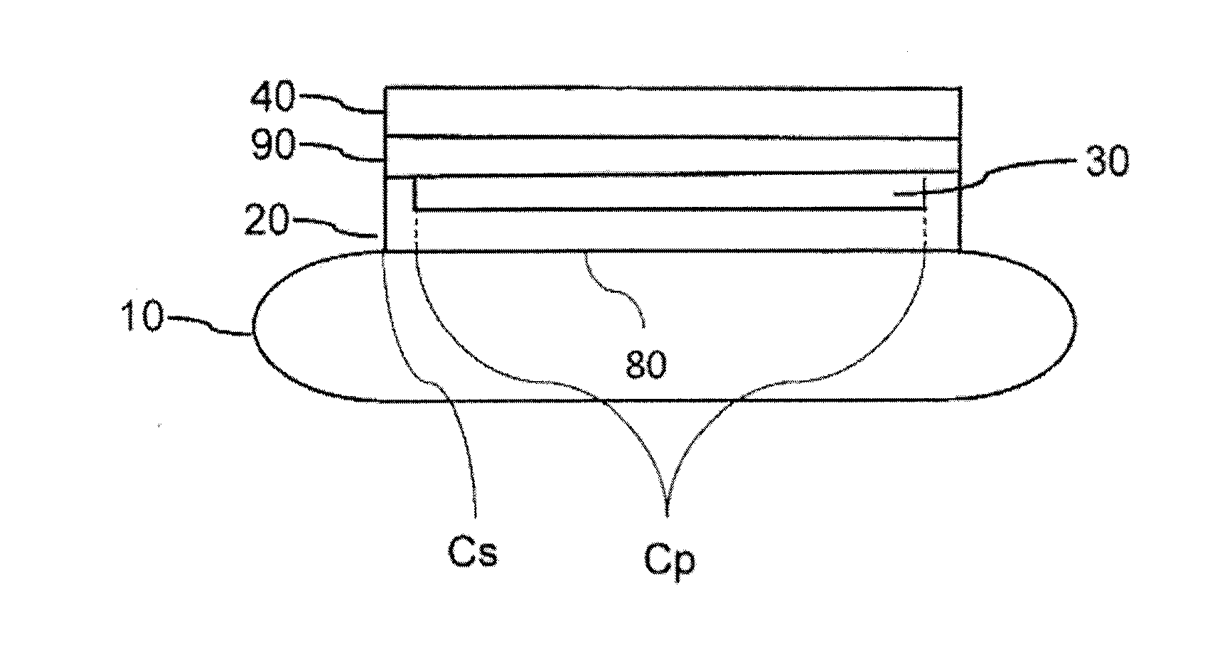
[0171]The second embodiment, illustrated in FIGS. 6A and 6B, differs from the first embodiment in that the donor substrate 50 comprises an additional layer 90, the additional layer 90 being in contact with the dielectric layer 30, the additional layer 90 having the same chemical composition as the covering layer 20.

[0172]For example, the additional layer 90 and the covering layer 20 comprise silicon oxide.

[0173]The additional layer 90 is formed directly on the donor substrate 50, before the dielectric layer 30.

[0174]The additional layer 90 may comprise a material, different from the materials of the dielectric layer 30, selected from the following materials: silicon oxide, silicon nitride or oxynitride, aluminium nitride, aluminium oxide, polycrystalline silicon and amorphous silicon.

[0175]Advantageously, the additional layer 90 is made from silicon oxide and its thickness is between 2 nm and 20 nm, for example, 7 nm.

[0176]When the donor substrate 50 is made from si...


PUM


Abstract

The disclosure relates to a process for manufacturing a composite structure, the process comprising the following steps: a) providing a donor substrate and a carrier substrate; b) forming a dielectric layer; c) forming a covering layer; d) forming a weakened zone in the donor substrate; e) joining the carrier substrate and the donor substrate via a contact surface having an outline; f) fracturing the donor substrate via the weakened zone, steps b) and e) being executed so that the outline is inscribed in the outline, and step c) being executed so that the covering layer covers the peripheral surface of the dielectric layer.

Description

CROSS-REFERENCE TO RELATED APPLICATIONS[0001]This application is a national phase entry under 35 U.S.C. §371 of International Patent Application PCT / FR2014 / 050666, filed Mar. 21, 2014, designating the United States of America and published as International Patent Publication WO 2014 / 154978 A1 on Oct. 2, 2014, which claims the benefit under Article 8 of the Patent Cooperation Treaty and under 35 U.S.C. §119(e) to French Patent Application Serial No. 1300738, filed Mar. 29, 2013, the disclosure of each of which is hereby incorporated herein in its entirety by this reference.TECHNICAL FIELD[0002]This disclosure relates to a method for manufacturing a composite structure. The disclosure also relates to a composite structure.BACKGROUND[0003]A method, illustrated in FIG. 1, for manufacturing a composite structure comprising, from its rear face to its front face, a supporting substrate 1, a covering layer 2, at least one dielectric layer 3 and a useful layer 4, and known from the prior art...

Claims


Application Information

Patent Timeline
IPC IPC(8): H01L21/762H01L21/02H01L27/12H01L29/06
CPCH01L21/76254H01L21/0217H01L29/0649H01L27/12H01L21/02164H01L21/62
Inventor KERDILES, SEBASTIENCHABANNE, GUILLAUMEBOEDT, FRANCOIS
Owner SOITEC
Why Eureka
Try Eureka