

Production method of semiconductor device, production method of display device, semiconductor device, production method of semiconductor element, and semiconductor element
- Summary
- Abstract
- Description
- Claims
- Application Information
AI Technical Summary
Benefits of technology
Problems solved by technology
Method used
Image

Examples
embodiment 1
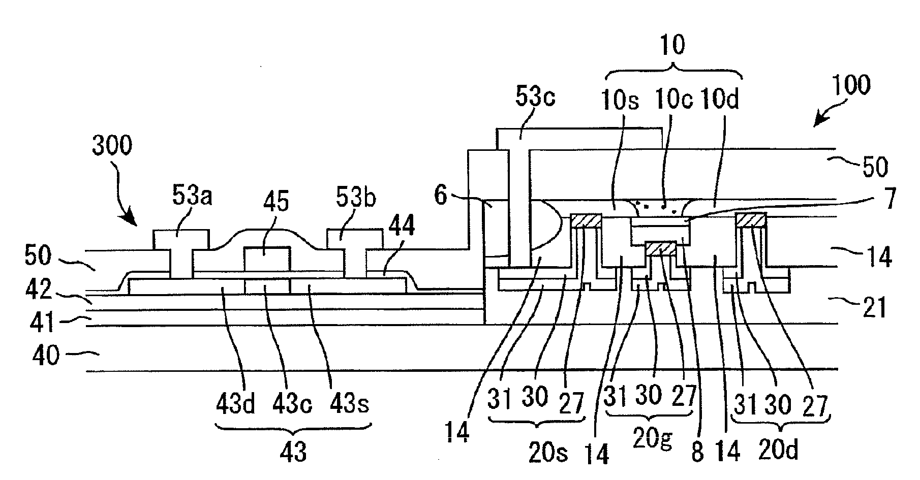
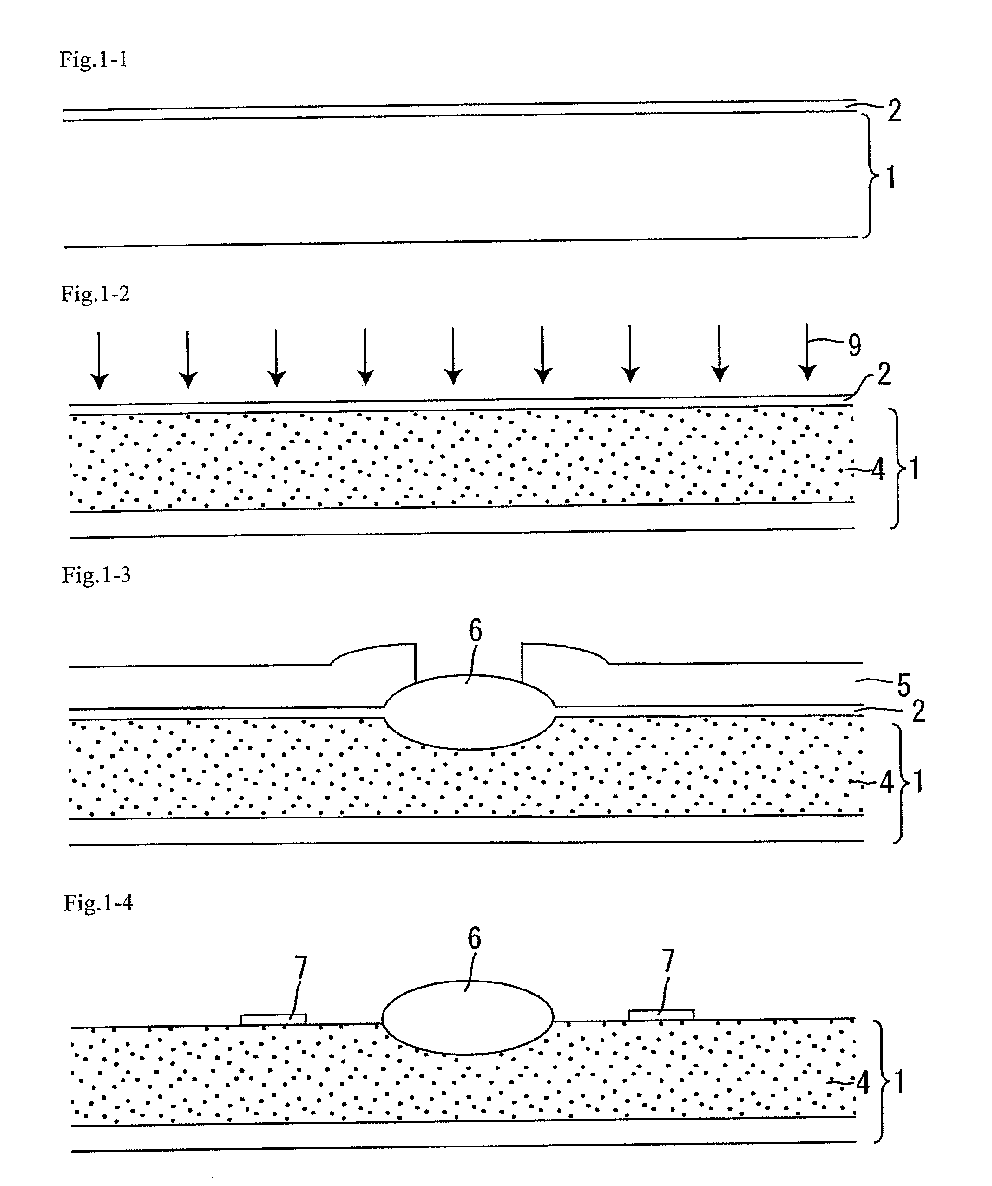
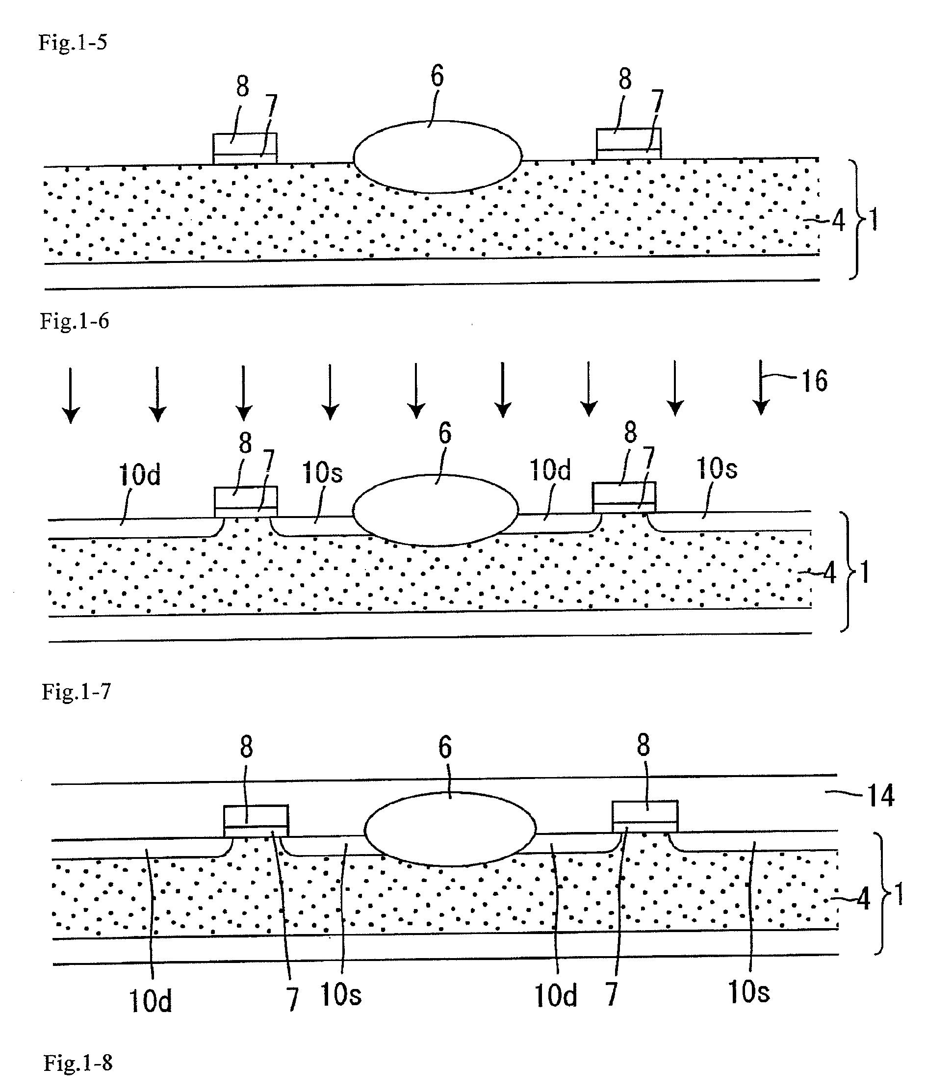
[0049]FIGS. 1-1 to 1-11, FIG. 2, and FIGS. 3-1 to 3-5 are cross-sectional views schematically showing production steps of a semiconductor device in accordance with Embodiment 1.
[0050](1) Production of single crystal silicon element (semiconductor element) (FIGS. 1-1 to 1-11), (2) production of substrate onto which single crystal silicon chip is transferred (FIGS. 2), and (3) production of semiconductor device (FIGS. 3-1 to 3-5) are mentioned below.
(1) Production of single crystal silicon element (FIGS. 1-1 to 1-11)
[0051]A thermal oxide film 2 is formed on a single crystal silicon substrate (single crystal silicon wafer) 1 by rapid oxidation and the like, first, as shown in FIG. 1-1.
[0052]Ions of boron 9 are implanted into the inside of the single crystal silicon substrate 1 by ion implantation, ion doping, and the like, as shown in FIG. 1-2. Successively, the implanted boron 9 ions are diffused and activated by thermal treatment, thereby forming a P-well region 4.
[0053]A silicon nit...
embodiment 2
[0072]The present Embodiment is the same as Embodiment 1, except that the thickness of the single crystal silicon layer 10 after being etched in such a way that the surface or inside of the LOCOS oxide film 6 is exposed (the thickness of the single crystal silicon layer just before forming the metal silicide) is 80 nm; and a Ti layer with a thickness of 20 nm (accounting for 25% of the thickness of the single crystal silicon layer) is used instead of the Ti layer 30 with a thickness of 30 nm. Only about 46 nm of the single crystal silicon layer is consumed for the Ti layer with a thickness of 20 nm, and so, the single crystal silicon layer with a thickness of about 34 nm remains.
[0073]Accordingly, the same operation and effects as in Embodiment 1 can be exhibited by the present Embodiment.
embodiment 3
[0074]The present Embodiment is the same as Embodiment 1, except that a cobalt layer (melting point: 1490° C.) with a thickness of 20 nm (accounting for 13% of the thickness of the single crystal silicon layer) is used instead of the Ti layer 30 with a thickness of 30 nm. Only about 70 nm of the single crystal silicon layer is consumed for the cobalt layer with a thickness of 20 nm, and so, the single crystal silicon layer with a thickness of about 80 nm remains.
[0075]Accordingly, the same operation and effects as in Embodiment 1 can be exhibited by the present Embodiment.
PUM
 Abstract
Description
Claims
Application Information