Signal tracing using on-chip memory for in-system post-fabrication debug

a technology of on-chip memory and in-system debugging, applied in the direction of error detection/correction, instruments, measurement devices, etc., can solve the problem that the initial run of a fabrication process for a particular design is rarely bug-fr

Active Publication Date: 2016-02-18
DUKE UNIV
View PDF10 Cites 18 Cited by
  • Summary
  • Abstract
  • Description
  • Claims
  • Application Information

AI Technical Summary

Problems solved by technology

Despite steady progress in pre-silicon verification methods and tools, first silicon—the initial run of a fabrication process for a particular design—is rarely bug-free.
However, the post-silicon debug of such highly integrated systems is one of the major challenges for the feasibility of commercial systems.

Method used


Image

  • Signal tracing using on-chip memory for in-system post-fabrication debug
  • Signal tracing using on-chip memory for in-system post-fabrication debug
  • Signal tracing using on-chip memory for in-system post-fabrication debug

Examples


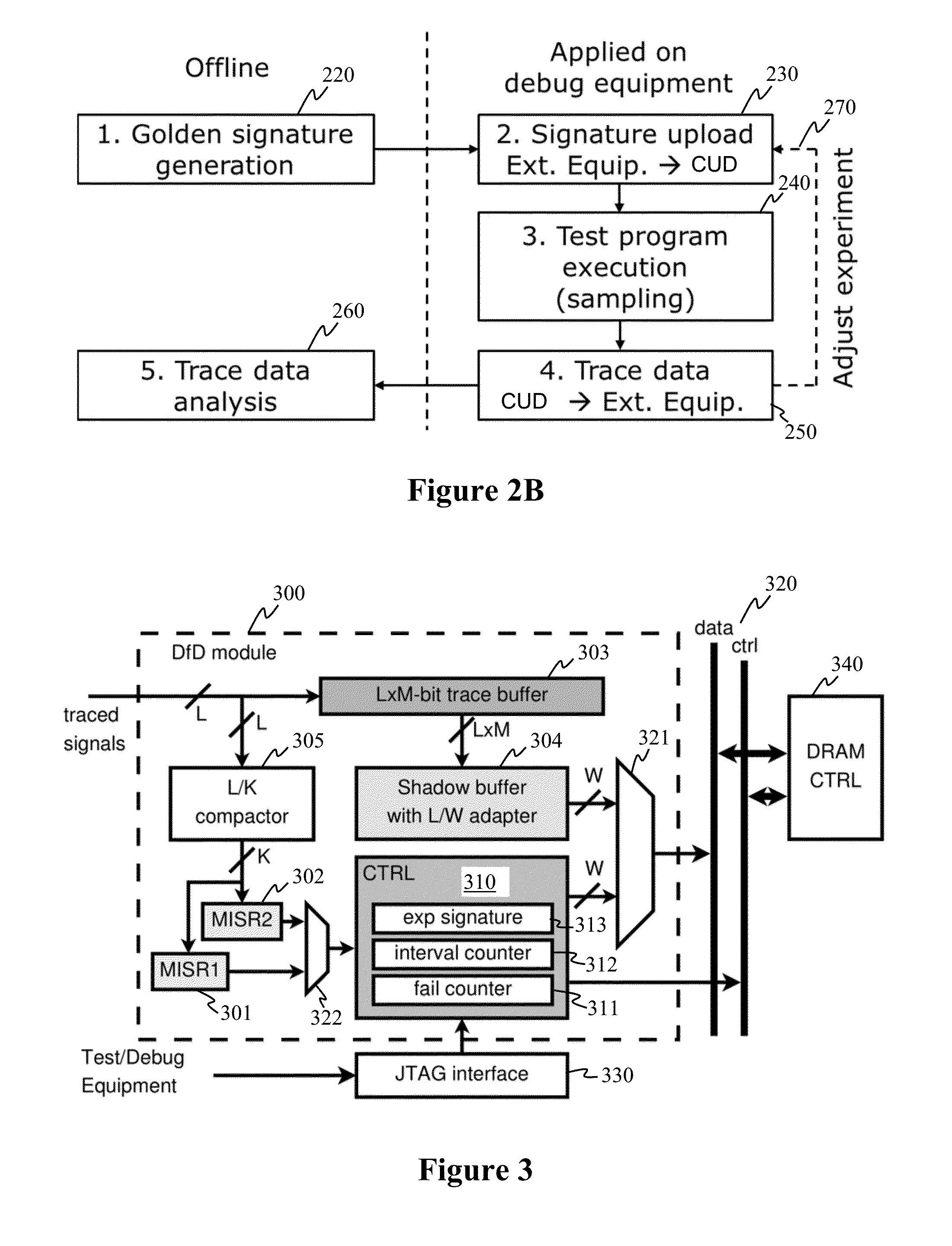
example dfd implementation

and Simulation

[0083]A Verilog RTL model of the architecture illustrated in FIG. 3 was created and synthesized using a 45 nm CMOS library. For the case L=K=32, S=32, and M=128, the synthesized circuit contained 8293 sequential and 8725 combinational gates. The standard-cell area of the design was 0.061 mm2, which is negligible for realistic chips. For instance, on a 25 mm2 die, the DfD circuitry would only occupy 0.24% of the die area.

[0084]In the first experiment, the functionality of the design was verified through simulation by using randomly generated data as an input stream. First, the expected signatures were calculated by applying the input stream to the MISR and recording the MISR's value every M cycles. In the second run, the full circuitry was simulated, where the DRAM was modeled as a Verilog module and initialized with the pre-calculated signatures. As expected, all intervals passed the comparison and no trace data was stored into the DRAM. In the third run, errors were i...


PUM


Abstract

A post-fabrication debug and on-line error checking framework for 2D- and 3D-ICs with integrated memories is described. A design-for-debug (DfD) architecture can include, for an IC with on-chip memory, a debug module connected to a functional bus of the IC. The debug module receives trace data for an interval, generates compact signatures based on the received data, and compares these signatures to expected signatures. Intervals containing erroneous trace data can be identified by the debug module and stored in on-chip memory. A single iteration of signal tracing for debug testing between automated test equipment and the IC is possible.

Description

[0001]This invention was made with government support under Federal Grant No. CCF-1017391 awarded by the National Science Foundation. The government has certain rights in the invention.BACKGROUND[0002]Modern CMOS technology has enabled the integration of hundreds of components in a single silicon chip. Recent advances in three-dimensional (3D) stacking of integrated circuits (ICs) and other components using through-silicon vias (TSVs) promise even denser integration in a single package. The production process flow generally involves pre-fabrication (or “pre-silicon”) simulations, followed by post-fabrication (or “post-silicon”) debug and validation. Despite steady progress in pre-silicon verification methods and tools, first silicon—the initial run of a fabrication process for a particular design—is rarely bug-free. However, the post-silicon debug of such highly integrated systems is one of the major challenges for the feasibility of commercial systems.[0003]Post-fabrication / post-si...

Claims


Application Information

Patent Timeline
Patent Type & Authority Applications(United States)
IPC IPC(8): G01R31/3177G06F11/34
CPCG06F11/348G01R31/3177G06F11/3636G01R31/31705G01R31/31703
Inventor DEUTSCH, SERGEJCHAKRABARTY, KRISHNENDU
Owner DUKE UNIV
Why Eureka
Try Eureka