Integrated circuit structure including fuse and method thereof

a technology of integrated circuits and fuse blades, which is applied in the direction of electrical equipment, semiconductor devices, semiconductor/solid-state device details, etc., can solve the problems of difficult to control the thickness of the formed protection layer precisely, the whole chip will be unusable, and the fuses can be selectively blown to repair or replace defective circuits

Active Publication Date: 2016-02-18
UNITED MICROELECTRONICS CORP
View PDF11 Cites 6 Cited by
  • Summary
  • Abstract
  • Description
  • Claims
  • Application Information

AI Technical Summary

Benefits of technology

[0010]As illustrated by the above, the present invention provides an integrated circuit structure including a fuse, and a method thereof, which forms a first dielectric layer directly on a fuse and then applies a dummy directly above the first dielectric layer. Therefore, the thickness of the first dielectric layer directly above the fuse can be controlled precisely by performing several etching processing steps using the dummy and the first dielectric layer as etching stop layers, as the dummy and the dielectric layer are composed of different materials.

Problems solved by technology

If a single metal link, a diode, or a MOS is broken down, the whole chip will be unusable.
When defects are found in a circuit, fuses can be selectively blown for repairing or replacing defective circuits.
Unfortunately, the thickness of the formed protection layer is difficult to be controlled precisely.

Method used


Image

  • Integrated circuit structure including fuse and method thereof
  • Integrated circuit structure including fuse and method thereof
  • Integrated circuit structure including fuse and method thereof

Examples


Embodiment Construction

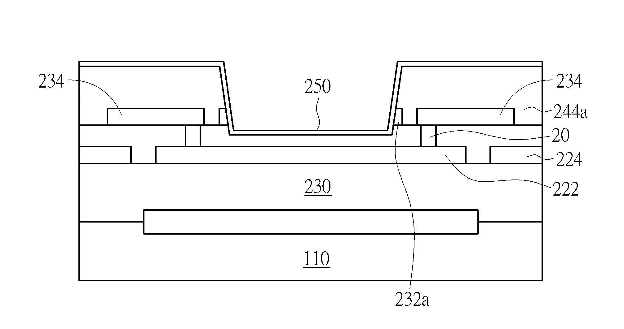
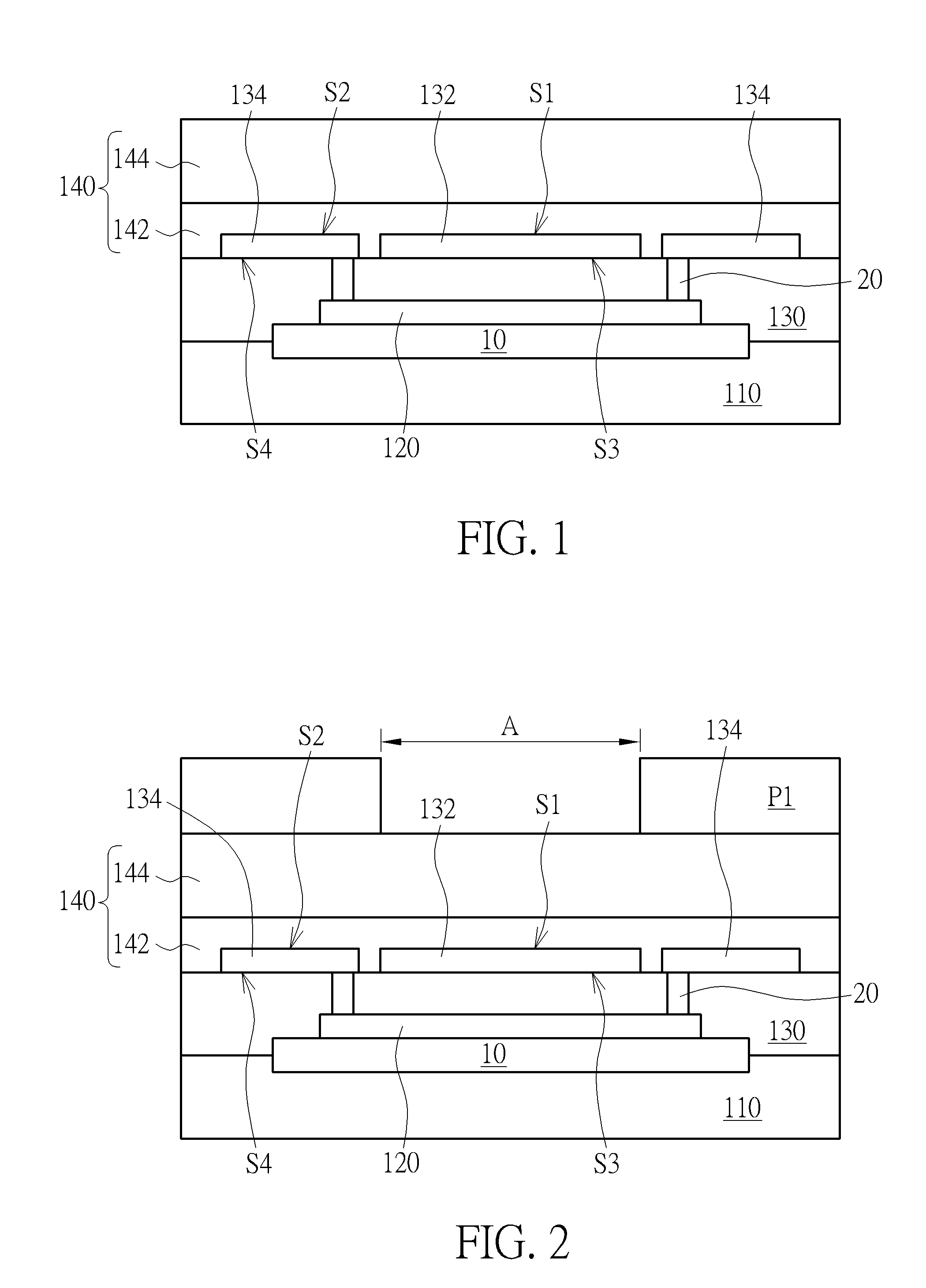
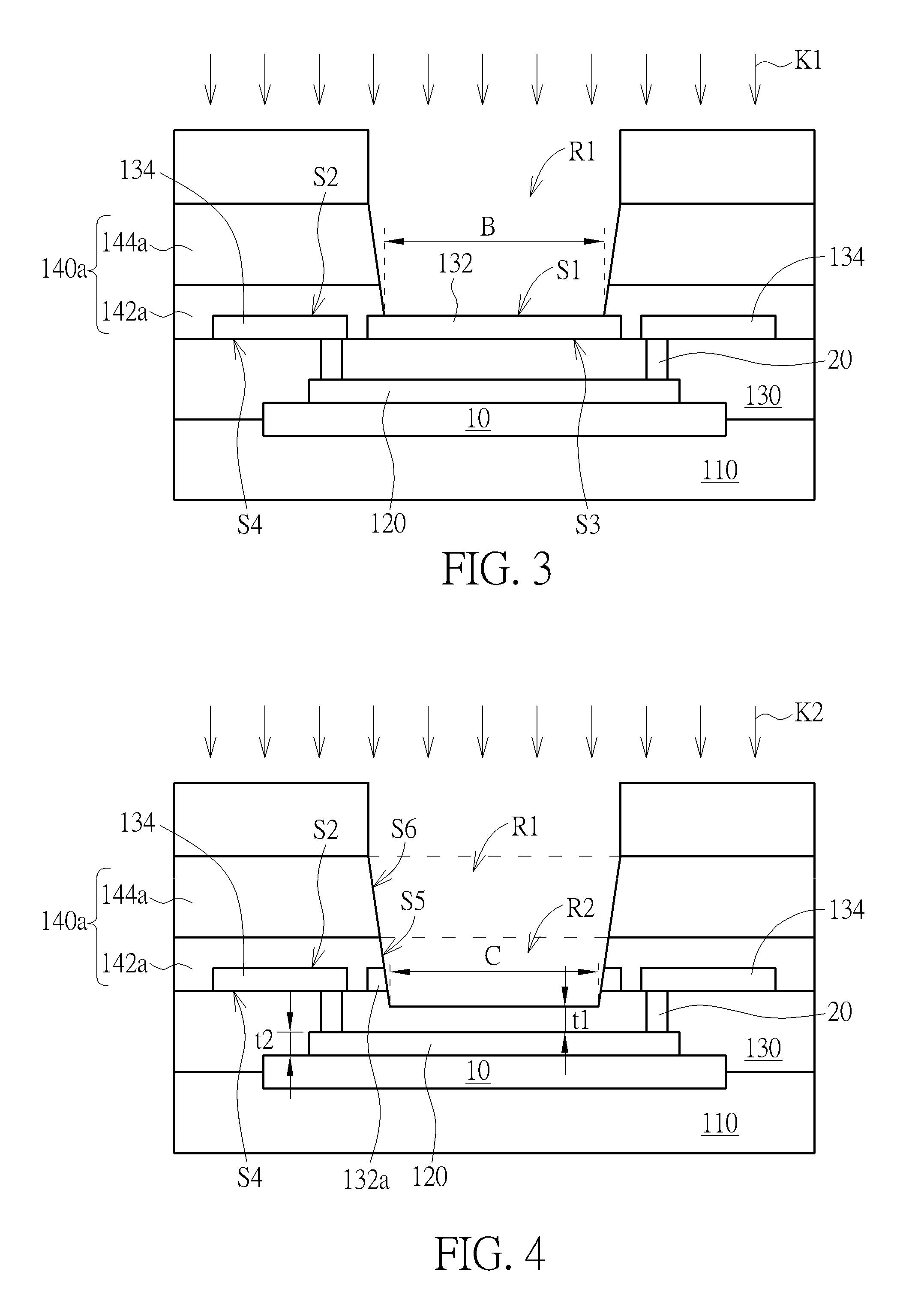
[0014]Embodiments of fuses such as a polysilicon fuse and a metal fuse are presented in the following. The present invention applying a dummy on a fuse to prevent over-etching can also be applied to other fuses. Furthermore, although only structures of a polysilicon fuse and a metal fuse are described in these embodiments, the polysilicon fuse and the metal fuse can be formed together with other structures such as transistors in the same processing steps. For example, the polysilicon fuse can be formed in the same process with a polysilicon gate of a transistor; the metal fuse can be formed in the same process with a metal interconnect for electrically connecting a transistor outwards.

[0015]FIGS. 1-5 schematically depict cross-sectional views of a method of an integrated circuit structure including a polysilicon fuse according to an embodiment of the present invention. As shown in FIG. 1, a substrate 110 is provided. The substrate 110 may be a semiconductor substrate such as a silic...


PUM


Abstract

An integrated circuit structure includes a fuse. The integrated circuit structure further includes a first dielectric layer and a patterned dummy. The fuse is disposed on a substrate. The first dielectric layer covers the fuse. The patterned dummy is disposed on the first dielectric layer and the patterned dummy has a first recess exposing a part of the first dielectric layer directly above the fuse. A method of forming the integrated circuit structure including a fuse is also provided.

Description

BACKGROUND OF THE INVENTION[0001]1. Field of the Invention[0002]The present invention relates generally to an integrated circuit structure including a fuse, and a method thereof, and more specifically to an integrated circuit structure including a fuse, and a method thereof, which applies a dummy right above the fuse.[0003]2. Description of the Prior Art[0004]As semiconductor processes become smaller and more complex, semiconductor components are more easily influenced by impurities. If a single metal link, a diode, or a MOS is broken down, the whole chip will be unusable. To treat this problem, fuses can be selectively blown to increase the yield of IC manufacturing.[0005]Fused circuits are redundant circuits of an IC. When defects are found in a circuit, fuses can be selectively blown for repairing or replacing defective circuits. In addition, fuses provide the function of programming circuits for various customized functions. Fuses are classified into two categories based on thei...

Claims


Application Information

Patent Timeline
Patent Type & Authority Applications(United States)
IPC IPC(8): H01L23/525H01L21/311H01L21/768H01L23/528H01L23/532
CPCH01L23/5256H01L23/528H01L23/53209H01L21/31111H01L21/31116H01L21/76897H01L23/53271H01L23/522H01L23/5258H01L2924/0002H01L2924/00
Inventor ROU, I-CHENG
Owner UNITED MICROELECTRONICS CORP
Why Eureka
Try Eureka