

Semiconductor device
a technology of semiconductor devices and resistors, applied in semiconductor devices, semiconductor/solid-state device details, diodes, etc., can solve the problems of cumbersomeness, special steps for forming ballast resistors, etc., and achieve the effect of improving esd tolerance and simple manner
- Summary
- Abstract
- Description
- Claims
- Application Information
AI Technical Summary
Benefits of technology
Problems solved by technology
Method used
Image

Examples
first embodiment
Variation of First Embodiment
[0070]Although the first embodiment above has described forming the ballast resistor on the source side of the transistor in the ESD discharge path, a ballast resistor can be formed on both the source side and the drain side.
[0071]This example will describe, as an example, forming a ballast resistor on both the source side and the drain side of N channel MOS transistor 604.
[0072]FIG. 6 is a diagram schematically illustrating the principle of an ESD protection element according to a variation of the first embodiment.
[0073]Referring to FIG. 6, the ESD protection element based on the variation of the first embodiment is shown having a configuration where a resistive component is added to both the source side and the drain side, as compared to the ESD protection element in the first embodiment.
[0074]Specifically, it is shown that a dummy gate electrode is provided on opposing sides of a transistor. The semiconductor device includes a plurality of gate electr...
second embodiment
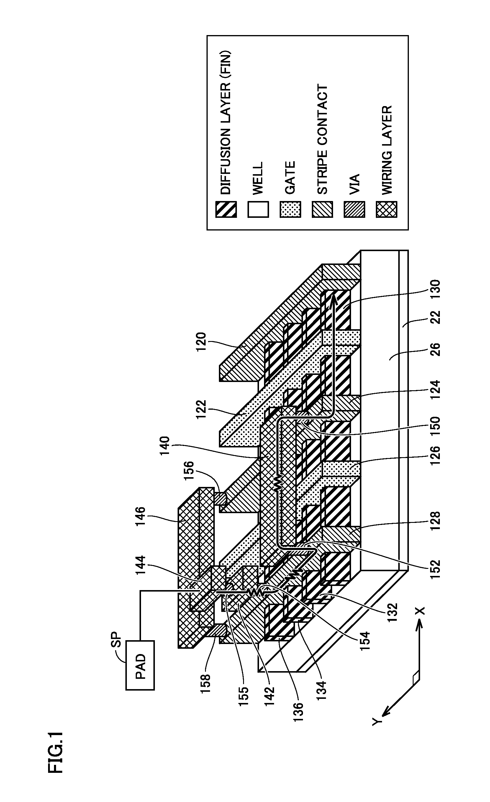
[0098]FIG. 9 is a diagram schematically illustrating the principle of an ESD protection element in a second embodiment.
[0099]Referring to FIG. 9, the ESD protection element based on the second embodiment is shown having a configuration where a resistive component is further added as compared to the ESD protection element in the first embodiment.
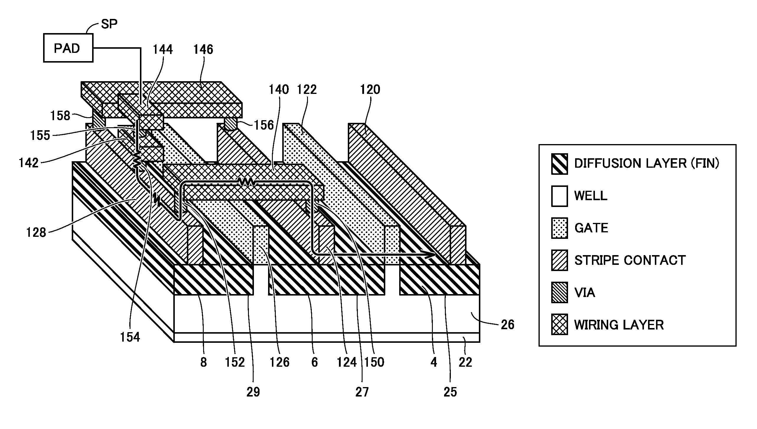
[0100]Specifically, it is shown that a plurality of dummy gate electrodes are provided. The semiconductor device includes the plurality of gate electrodes 122, 125 and 126 of a transistor formed on well 26 of semiconductor substrate 22, and the plurality of stripe contacts 120, 123, 124 and 128 formed along the length direction (Y direction) of gate electrodes 122, 125 and 126 so as to form a source and a drain of the transistor. Gate electrode 122, and stripe contacts 120 and 123 provided on opposing sides of gate electrode 122 form a conductive transistor. Although not shown, the reference potential (ground voltage VSS by way of example) is...
third embodiment
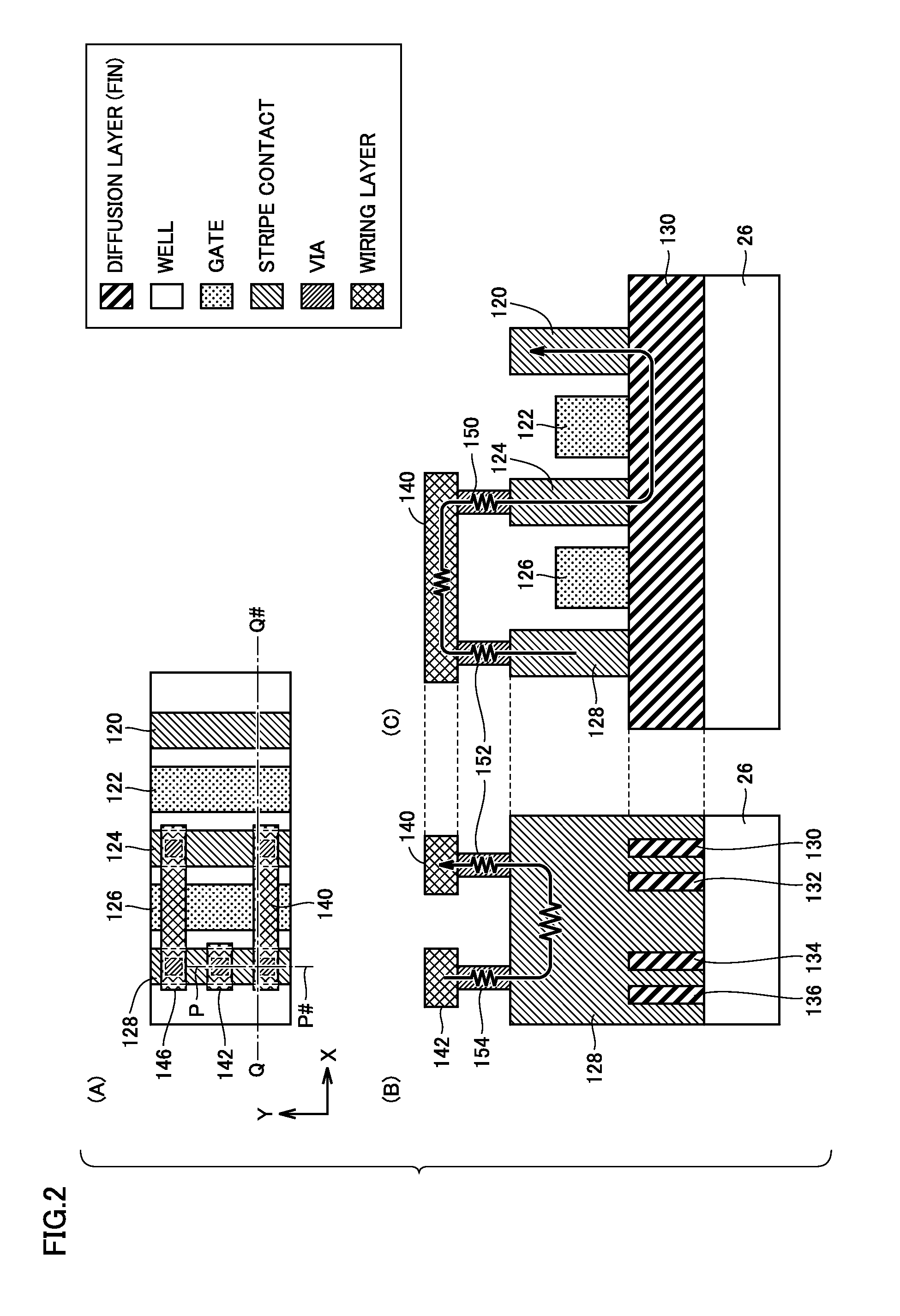
[0112]FIG. 10 is a diagram schematically illustrating the principle of an ESD protection element in a third embodiment.
[0113]Referring to FIG. 10, a planar FET is shown. The stripe contacts can be utilized in this planar FET as well.
[0114]Well 26 is formed on semiconductor substrate 22, and well 26 is provided with diffusion regions 25, 27 and 29 for forming a source and a drain.
[0115]The semiconductor device includes the plurality of gate electrodes 122 and 126 of a transistor formed on well 26 of semiconductor substrate 22, and the plurality of stripe contacts 120, 124 and 128 formed along the length direction (Y direction) of gate electrodes 122 and 126 so as to form a source and a drain of the transistor. Gate electrode 122, and stripe contacts 120 and 124 provided on opposing sides of gate electrode 122 form a conductive transistor. Although not shown, the reference potential (ground voltage VSS by way of example) is applied to stripe contact 120 of the conductive transistor. G...
PUM
 Abstract
Description
Claims
Application Information