Alignment apparatus and substrate processing apparatus

Active Publication Date: 2016-03-17
TOKYO ELECTRON LTD
View PDF4 Cites 6 Cited by
  • Summary
  • Abstract
  • Description
  • Claims
  • Application Information

AI Technical Summary

Benefits of technology

The disclosure provides a way to accurately detect a mark on the back of a wafer and estimate its war probabilistically using a simple apparatus. By controlling the position of the mounting unit based on changes in brightness, the apparatus can automatically focus on the mark and detect it accurately. This technique avoids the need for a camera that is actively focused on the subject, making it easier to estimate the warUS Patent text describes a technique to accurately detect the location of an alignment mark on a wafer and determine its war Ocean variations in brightness can be used to control the position of the apparatus, ensuring accurate detection of the mark. The technique is simple and does not require an actively focused camera.

Problems solved by technology

In that case, if the camera does not have a function of automatically controlling a focus, i.e., a so-called autofocus function, the camera is not focused on the alignment mark and the circumferential edge of the wafer, which makes the obtained image blurry.
As a consequence, the alignment mark cannot be detected, and the detection accuracy of the position of the circumferential edge of the wafer may deteriorate.
However, such a camera is expensive, which increases a manufacturing cost of the alignment apparatus.
However, the configuration of the movable camera and the displacement sensor results in scaling up of the alignment apparatus.
However, the alignment apparatus of Japanese Patent Application Publication No. 2009-129944 is disadvantageous in that the apparatus configuration may be scaled up due to the presence of the displacement sensor.
Further, the alignment apparatus of Japanese Patent Application Publication No. 2009-129944 does not include a camera, and cannot solve the above-described problem.

Method used


Image

  • Alignment apparatus and substrate processing apparatus
  • Alignment apparatus and substrate processing apparatus
  • Alignment apparatus and substrate processing apparatus

Examples


Embodiment Construction

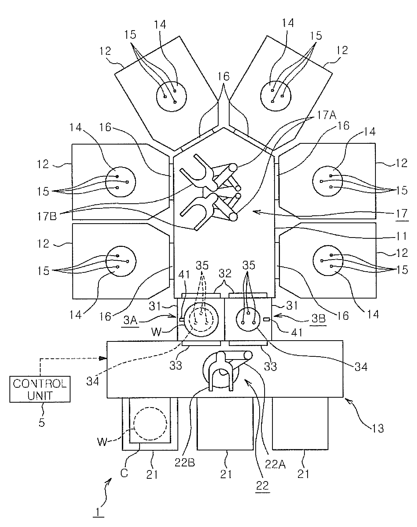
[0027]A substrate processing apparatus 1 according to an embodiment will be described with reference to the schematic top view of FIG. 1. The substrate processing apparatus 1 that is a semiconductor manufacturing apparatus performs plasma treatment on wafers W one at a time. A wafer W has a diameter of, e.g., 450 mm. The substrate processing apparatus 1 includes, when viewed from the top, elongated pentagonal transfer module 11; six processing modules 12 arranged radially around the transfer module 11 and connected to the transfer module 11; a loader module 13 disposed to face the transfer module 11; and two load-lock modules 3A and 3B disposed between the transfer module 11 and the loader module 13.

[0028]Each of the processing modules 12 has a vacuum chamber. Provided in the vacuum chamber is a stage 14 for mounting thereon the wafer W. In FIG. 1, a reference numeral 15 denotes elevating pins for transferring the wafer W to and from a first wafer transfer unit 17 to be described la...


PUM


Abstract

An alignment apparatus for aligning a wafer includes a mounting unit, an imaging unit, an elevation unit, and a controlling unit. The control unit outputs a control signal for controlling the elevation unit such that a luminance variation between the outer side and the inner side of the wafer obtained by the imaging unit becomes the same as a luminance variation obtained when the imaging unit is focused, for estimating a warpage state of the wafer based on an amount of relative movement of the imaging unit and the mounting unit with respect to a relative height position of the imaging unit and the mounting unit obtained when the imaging unit is focused on a reference wafer having no warpage, and for detecting the alignment mark of the wafer by the imaging unit by rotating the mounting unit in a state where the imaging unit is focused.

Description

CROSS-REFERENCE TO RELATED APPLICATIONS[0001]This application claims priority to Japanese Patent Application No. 2014-188758 filed on Sep. 17, 2014, the entire contents of which are incorporated herein by reference.FIELD OF THE INVENTION[0002]The disclosure relates to an alignment apparatus for optically detecting an alignment mark by imaging a substrate and a substrate processing apparatus including the alignment apparatus.BACKGROUND OF THE INVENTION[0003]In a semiconductor manufacturing apparatus that is a substrate processing apparatus, a semiconductor wafer (hereinafter, referred to as “wafer”) that is a substrate is transferred to a processing module by a transfer unit and subjected to processing. Before the wafer is transferred to the processing module by the transfer unit, the wafer may be transferred to an alignment apparatus so that a direction and a position of a circumferential edge thereof can be detected. The transfer unit receives the wafer from the alignment apparatus...

Claims


Application Information

Patent Timeline
IPC IPC(8): G06T7/00
CPCG06T7/0044G06T7/0004G06T7/0085G06T2207/30204G06T7/0069G06T2207/10152G06T2207/30148G06T7/0024G05B2219/37224G05B2219/45031G05B2219/45178G05B2219/49112H01L21/681
Inventor KODAMA, TOSHIAKIYAMAUCHI, TORU
Owner TOKYO ELECTRON LTD
Why Eureka
Try Eureka