Semiconductor device

a technology of semiconductor devices and semiconductor elements, applied in semiconductor devices, semiconductor/solid-state device details, electrical apparatus, etc., can solve the problems of increasing the misalignment of the printed circuit board b>109/b> itself, the difficulty of bonding the semiconductor element, and the significant increase in the misalignment of the printed circuit board b>109/b>, so as to improve the yield rate of the assembled power semiconductor module and reduce the failure of connection

Inactive Publication Date: 2016-03-17
FUJI ELECTRIC CO LTD
View PDF0 Cites 11 Cited by
  • Summary
  • Abstract
  • Description
  • Claims
  • Application Information

AI Technical Summary

Benefits of technology

[0015]This problem can be solved by increasing the inner diameter of the through-hole 113 of the printed circuit board 109 to be larger than the inner diameter of the external terminal 110. By doing so, the influence of inclination or the like of the external terminal 110 can be reduced. However, in this case, a new problem occurs in that the misalignment of the printed circuit board 109 itself increases.
[0017]In order to solve the problem, according to an aspect of the present invention, there is provided a semiconductor device including: an insulating substrate which has on a principal surface thereof a circuit plate; a semiconductor element which is fixed to the circuit plate; an external terminal, one end of which is fixed to the circuit plate; and a printed circuit board which has a through-hole, through which the external terminal passes, and faces the principal surface of the insulating substrate. A rigidity of a peripheral region of the through-hole is lower than a rigidity of other regions.
[0018]According to the invention, even when an external terminal inserted in a recess of a DCB substrate that forms a power semiconductor module is inclined slightly, it is possible to decrease connection failure which can cause floating and misalignment of a printed circuit board. Due to this, it is possible to improve the yield rate of the assembled power semiconductor module.

Problems solved by technology

Thus, it is difficult to bond the semiconductor element 106 and the post electrode 108 by the bonding material 107 such as a solder and manufacturing defects may occur.
However, in this case, a new problem occurs in that the misalignment of the printed circuit board 109 itself increases.
Due to this, an increase in misalignment of the printed circuit board 109 is a significant problem in manufacturing.

Method used


Image

  • Semiconductor device
  • Semiconductor device
  • Semiconductor device

Examples


Embodiment Construction

[0026]Hereinafter, preferred embodiments (practical examples) of the present invention will be described with reference to the drawings.

[0027]The same constituent elements throughout the embodiments will be denoted by the same reference numerals and redundant description thereof will not be provided.

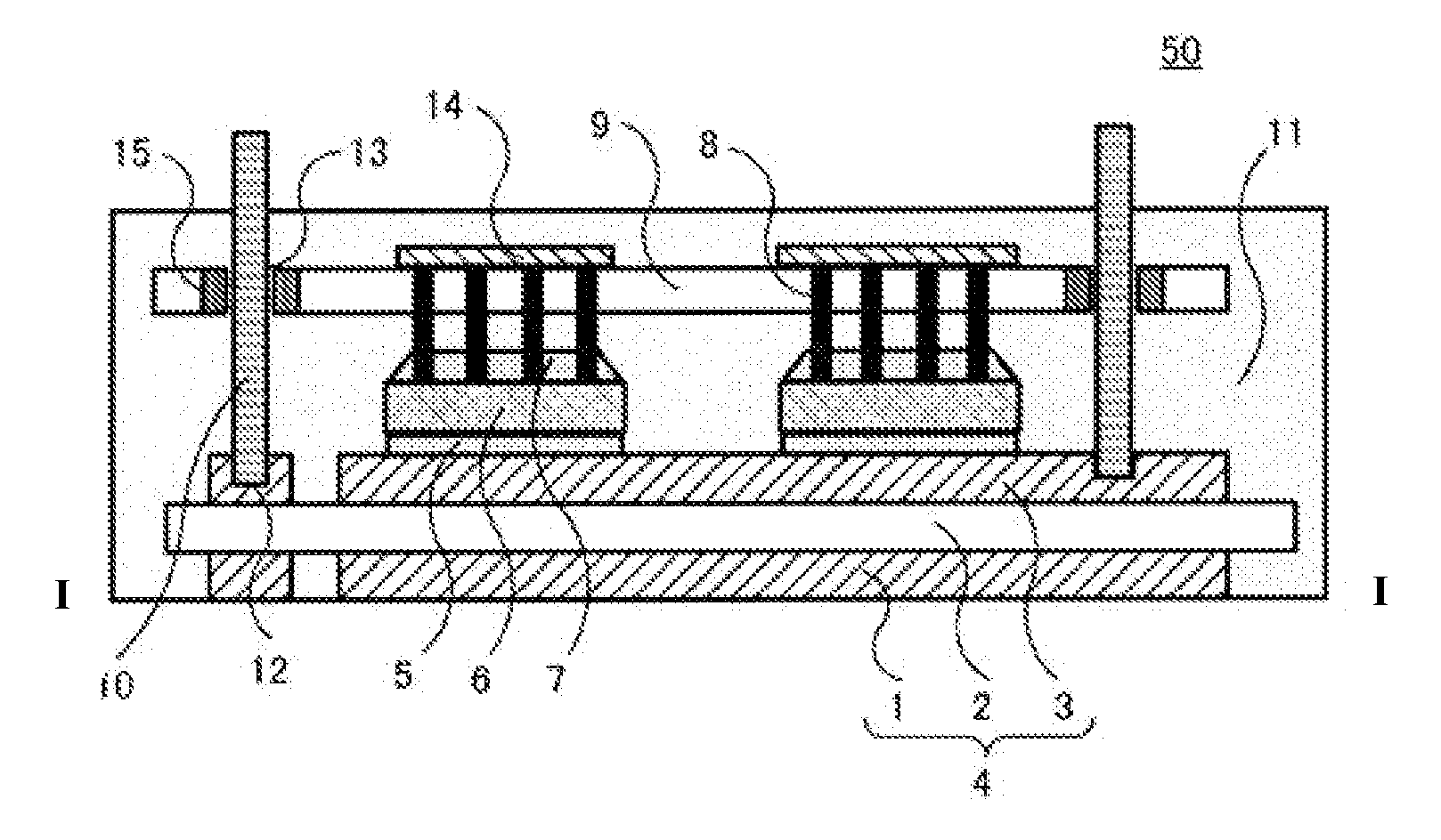
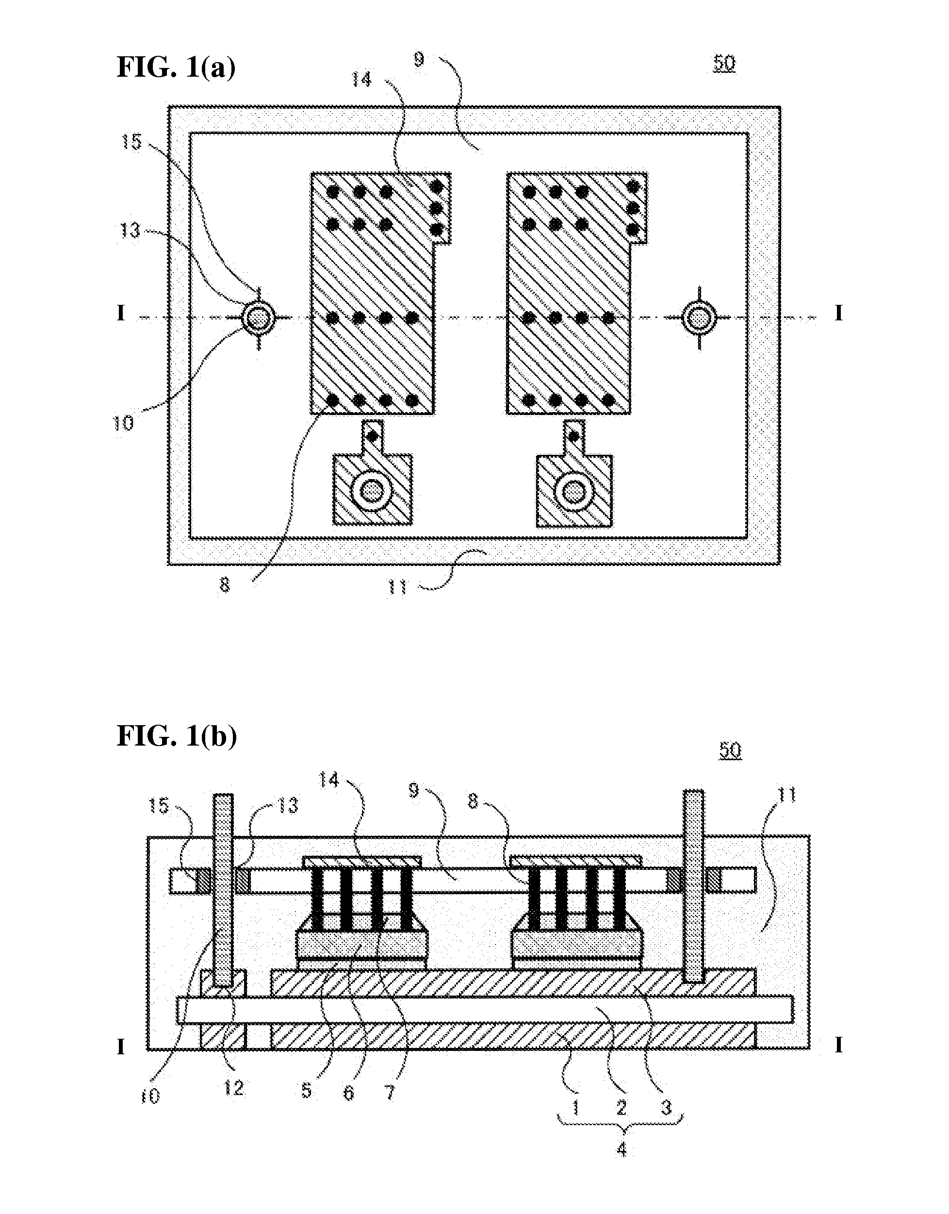
[0028]FIGS. 1(a) and 1(b) are a plan view and a cross-sectional view of a semiconductor device according to a first embodiment, respectively.

[0029]FIG. 1(b) is a cross-sectional view of a main part taken along line I-I in FIG. 1(a).

[0030]The illustrated power semiconductor module (semiconductor device) 50 has a structure in which a DCB substrate 4 and a printed circuit board 9 facing the DCB substrate 4 are integrated by a sealing resin 11. Moreover, a semiconductor element 6 is fixed to a circuit plate 3 positioned on a principal surface of the DCB substrate 4.

[0031]The DCB substrate 4 includes an insulating substrate 2, a heat-radiating plate 1 formed on a rear surface of the insulatin...


PUM


Abstract

A semiconductor device includes an insulating substrate having a circuit plate on a principal surface thereof; a semiconductor element fixed to the circuit plate; an external terminal having one end fixed to the circuit plate; and a printed circuit board facing the principal surface of the insulating substrate, and having a through-hole for passing through the external terminal. A rigidity of a peripheral region of the through-hole is lower than a rigidity of other regions.

Description

CROSS-REFERENCES TO RELATED APPLICATIONS[0001]The present application is a Continuation Application of PCT International Application No. PCT / JP2014 / 062389 filed May 8, 2014, and claiming priority from Japanese Application No. 2013-118495 filed Jun. 5, 2013, the disclosure of which is incorporated herein.TECHNICAL FIELD[0002]The present invention relates to a semiconductor device, and more particularly, to a power semiconductor module on which a power semiconductor element is mounted.BACKGROUND ART[0003]FIGS. 4(a) and 4(b) are a plan view and a cross-sectional view of a power semiconductor module according to a related art, respectively. FIG. 4(b) is a cross-sectional view of a main part taken along line in FIG. 4(a).[0004]In FIGS. 4(a) and 4(b), a power semiconductor module 500 includes a direct copper bonding (DCB) substrate 104, a semiconductor element 106, a post electrode 108, an external terminal 110, and a printed circuit board 109.[0005]The DCB substrate 104 has a circuit pla...

Claims


Application Information

Patent Timeline
Patent Type & Authority Applications(United States)
IPC IPC(8): H01L23/053H01L23/08
CPCH01L23/08H01L23/053H01L24/01H01L2924/1305H01L2924/13055H01L2924/13091H01L25/072H01L23/3121H01L2924/181H01L2924/00H01L2924/00012H01L25/07H01L25/18
Inventor NASHIDA, NORIHIRONAKAMURA, YOKO
Owner FUJI ELECTRIC CO LTD
Why Eureka
Try Eureka