Patterning method and semiconductor structure

a technology of semiconductor structure and pattern pitch, applied in the field of integrated circuits, can solve problems such as difficult control of critical dimension uniformity, and achieve the effect of improving critical dimension uniformity and small pattern pitch

Active Publication Date: 2016-03-24
MACRONIX INT CO LTD
View PDF1 Cites 5 Cited by
  • Summary
  • Abstract
  • Description
  • Claims
  • Application Information

AI Technical Summary

Benefits of technology

[0005]The invention provides a patterning method, adapted for obtaining smaller pattern pitch and critical dimension and for aligning the formed patterns with each other, so as to overcome misalignment and improve critical dimension uniformity.

Problems solved by technology

However, misalignment may occur in a pattern formed by such a method, and because of the difficulty of the fabrication, it is also hard to control the critical dimension uniformity.

Method used


Image

  • Patterning method and semiconductor structure
  • Patterning method and semiconductor structure
  • Patterning method and semiconductor structure

Examples


Embodiment Construction

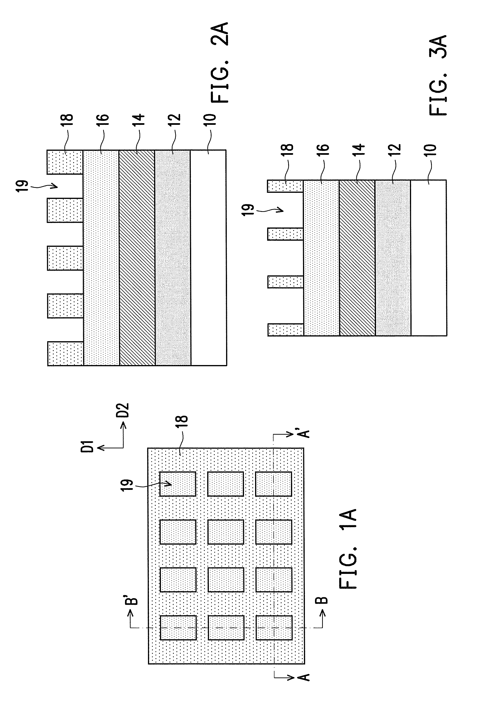
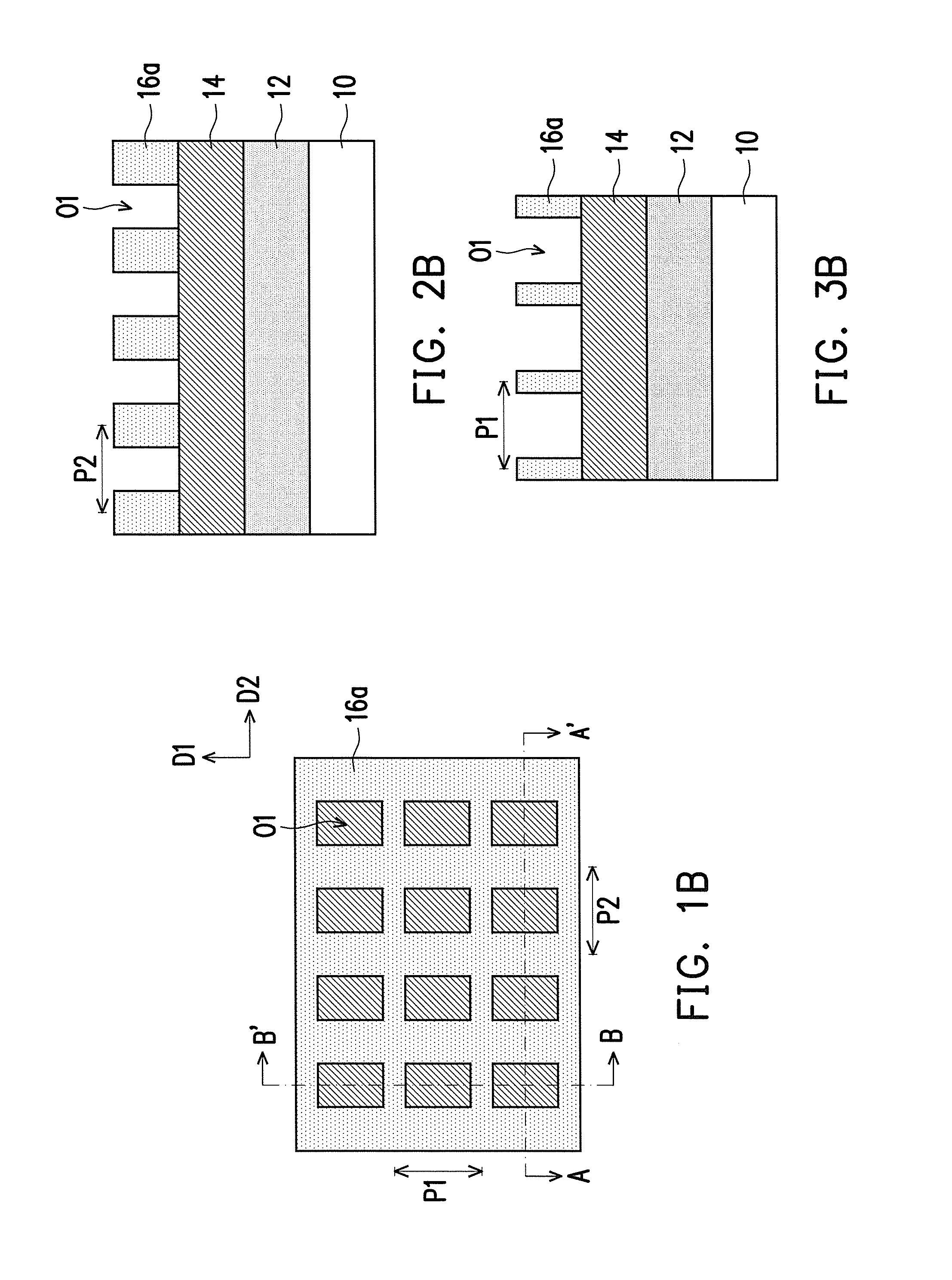
[0033]FIG. 1A to FIG. 1E are schematic top views showing a patterning method according to an embodiment of the invention. FIG. 2A to FIG. 2E are schematic cross-sectional views taken along the line A-A′ of FIG. 1A to FIG. 1E. FIG. 3A to FIG. 3E are schematic cross-sectional views taken along the line B-B′ of FIG. 1A to FIG. 1E.

[0034]With reference to FIG. 1A to FIG. 3A, a substrate 10 is provided, and a material layer 12 is formed on the substrate 10. The substrate 10 is a semiconductor substrate, a semiconductor compound substrate, or a semiconductor over insulator (SOI) substrate, for example. The semiconductor is IVA group atoms, such as silicon or germanium, for example. The semiconductor compound is formed of IVA group atoms, such as silicon carbide or silicon germanium, or formed of IIIA group atoms and VA group atoms, such as gallium arsenide, for example. The material layer 12 is a conductor layer, and a material thereof is metal, polysilicon, polycide, or metal silicide, fo...


PUM


Abstract

A patterning method is provided. A substrate including a material layer thereon is provided. A patterned hard mask layer, having a plurality of first holes, is formed on the material layer. Afterward, a mask layer, including a plurality of line pattern masks extending in a direction and dividing each first hole into a second hole and a third hole, is formed. The material layer is patterned using the patterned hard mask layer and the mask layer as masks to form a patterned material layer having a plurality of fourth and fifth holes. Furthermore, a semiconductor structure is provided.

Description

BACKGROUND OF THE INVENTION[0001]1. Field of the Invention[0002]The invention relates to an integrated circuit and more particularly relates to a patterning method and a semiconductor structure.[0003]2. Description of Related Art[0004]The conventional lithography techniques, such as ArF immersion lithography, can only form pitch of about 76 nm in one single process. If smaller pitch is desired, secondary lithography and etching processes are needed. However, misalignment may occur in a pattern formed by such a method, and because of the difficulty of the fabrication, it is also hard to control the critical dimension uniformity. Thus, a method for obtaining smaller pattern pitch using the existing lithography process is required.SUMMARY OF THE INVENTION[0005]The invention provides a patterning method, adapted for obtaining smaller pattern pitch and critical dimension and for aligning the formed patterns with each other, so as to overcome misalignment and improve critical dimension un...

Claims


Application Information

Patent Timeline
Patent Type & Authority Applications(United States)
IPC IPC(8): H01L21/308H01L21/311
CPCH01L21/3088H01L21/3086H01L21/31105H01L21/31127H01L21/32139
Inventor YANG, CHIN-CHENG
Owner MACRONIX INT CO LTD
Why Eureka
Try Eureka