Display panel and method of manufacturing the same

a technology of display panel and manufacturing method, which is applied in the direction of conductive pattern formation, instruments, coatings, etc., can solve the problems of difficult to form the conductive path in the desired shape, unfavorable light control material deterioration or degeneration, and process may take a long time. , to achieve the effect of improving stability, preventing deterioration or degeneration of light control material, and uniform thickness and width

Active Publication Date: 2016-03-31
LG DISPLAY CO LTD
View PDF13 Cites 17 Cited by
  • Summary
  • Abstract
  • Description
  • Claims
  • Application Information

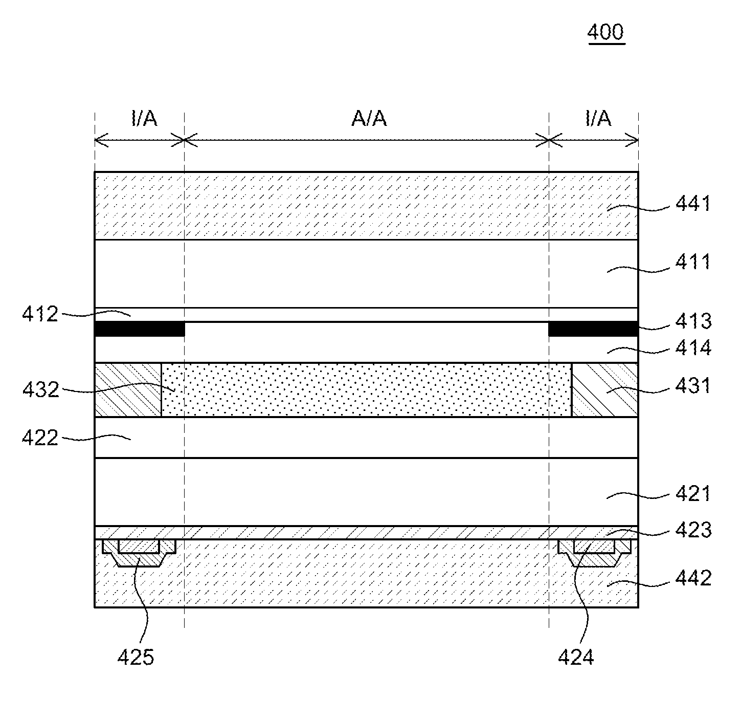
AI Technical Summary

Benefits of technology

[0008]An advantage of the present invention is directed to provide a display device including a conductive path formed by an inkjet printing with improved stability.
[0009]Additional features and advantages of the invention will be set forth in the description which follows, and in part will be apparent from the description, or may be learned by practice of the invention. These and other advantages of the invention will be realized and attained by the structure particularly pointed out in the written description and claims hereof as well as the appended drawings.
[0010]To achieve these and other advantages and in accordance with the purpose of the present invention, as embodied and broadly described, a display device may, for example, include a display panel including a light controlling material between a lower substrate and an upper substrate; a TFT layer on an upper surface of the lower substrate; and an inkjet-printed metal pattern on a lower surface of the lower substrate, the inkjet-printed metal pattern having substantially uniform thickness and width and serving as a conductive path in the display panel, wherein the inkjet-printed metal pattern is cured at a temperature in consideration of substantially preventing deterioration or degeneration of the light controlling material.
[0011]In another aspect of the present

Problems solved by technology

However, a solvent needs to be removed to solidify the metallic ink on the substrate, and this process may take a long time.
Also, an undesirable amount of metal may be lost while solidifying the metallic i

Method used


Image

  • Display panel and method of manufacturing the same
  • Display panel and method of manufacturing the same
  • Display panel and method of manufacturing the same

Examples


Embodiment Construction

[0027]Advantages and features of the present invention, and methods for accomplishing the same will be more clearly understood from exemplary embodiments described below with reference to the accompanying drawings. However, the present invention is not limited to the exemplary embodiments but may be described in the present disclosure. The exemplary embodiments are provided only to complete disclosure of the present invention and to fully provide a person having ordinary skill in the art to which the present invention pertains with the category of the invention, and the present invention will be defined by the appended claims.

[0028]The shapes, sizes, ratios, angles, numbers, and the like illustrated in the accompanying drawings for describing the exemplary embodiments of the present invention are merely examples, and the present invention is not limited thereto.

[0029]Like reference numerals generally denote like elements throughout the present specification.

[0030]In the following de...


PUM


Abstract

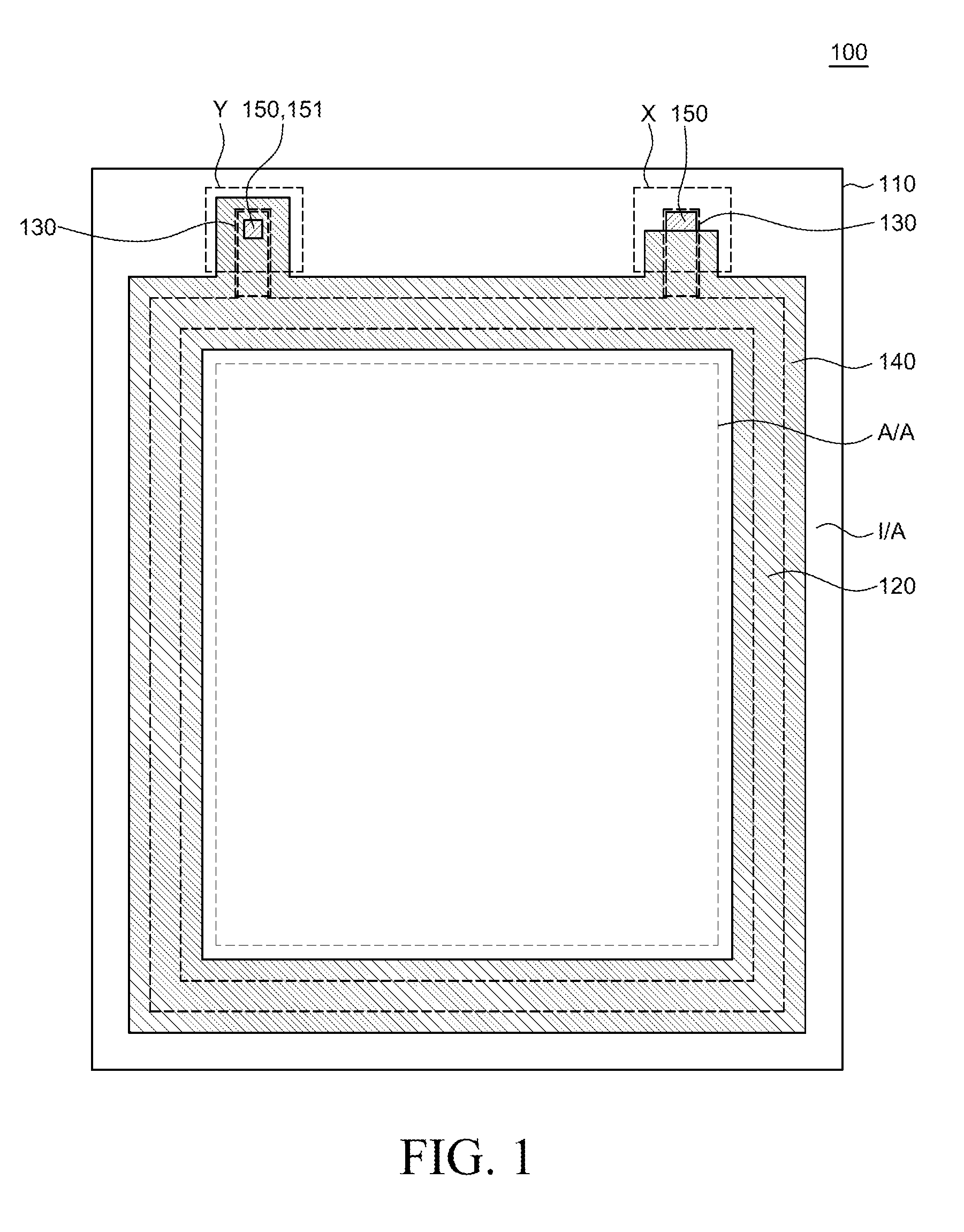
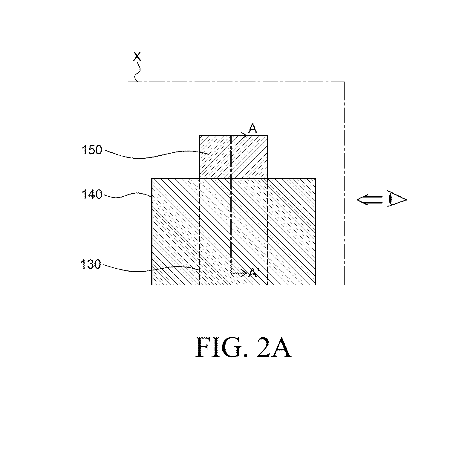
Provided is a display panel including a loop-shaped conductive path which is manufactured by performing a conductive ink jetting process and a high-degree vacuum removal process to effectively vaporizing a solvent in a conductive ink line at lower temperature than the boiling point at atmospheric pressure of the solvent. The conductive path manufactured as such does not allow a stain or a trace, such as a pull-back region, to be left around the conductive path. Thus, it is possible to obtain the loop-shaped conductive path having an initially intended design without being damaged during a process.

Description

[0001]This application claims the priority of Korean Patent Application Nos. 10-2014-0129282 filed on Sep. 26, 2014 and 10-2015-0028572 filed on Feb. 27, 2015, in the Korean Intellectual Property Office, the disclosures of which are incorporated herein by reference for all purposes as if fully set forth herein.BACKGROUND OF THE INVENTION[0002]1. Field of the Invention[0003]The present invention relates to a display device and a method for manufacturing the same, and more particularly, to a display device including a conductive path and a method for manufacturing the same.[0004]2. Discussion of the Related Art[0005]A method for forming a metal wire having a continuous and integrated loop shape includes the use of a metallic ink and performing inkjet printing. Using the inkjet printing, a conductive pattern can be formed on a substrate by adjusting a position, a moving speed, and a jet velocity of a nozzle that dispenses the metallic ink.[0006]However, a solvent needs to be removed to...

Claims


Application Information

Patent Timeline
IPC IPC(8): G06F3/041G06F3/044G06F3/045H05K1/02H05K1/09H05K3/12
CPCG06F3/0412G06F3/044G06F3/045G06F2203/04106H05K1/092H05K3/125G06F2203/04103H05K1/0296G02F1/13338G06F2203/04107G02F1/136295H05K1/0306H05K1/0393H05K1/097H05K3/1283H05K3/282H05K2201/026H05K2201/0323H05K2201/0326H05K2201/098H05K2201/10128H05K2203/0514H05K2203/085
Inventor KONG, SUNBAEPARK, JEONGKWEONPARK, CHANRYU, KYENGBAEKJO, HEUNGJU
Owner LG DISPLAY CO LTD
Why Eureka
Try Eureka