
Three-dimensional non-volatile ferroelectric random access memory

a non-volatile, ferroelectric technology, applied in the direction of basic electric elements, semiconductor devices, electrical equipment, etc., can solve the problems of high cost of ferroelectric devices and thus less competitive in most cases, except for certain niche applications, and achieve high storage densities.

Inactive Publication Date: 2016-04-28
PENG HAIBING
View PDF5 Cites 67 Cited by
  • Summary
  • Abstract
  • Description
  • Claims
  • Application Information

AI Technical Summary

Benefits of technology

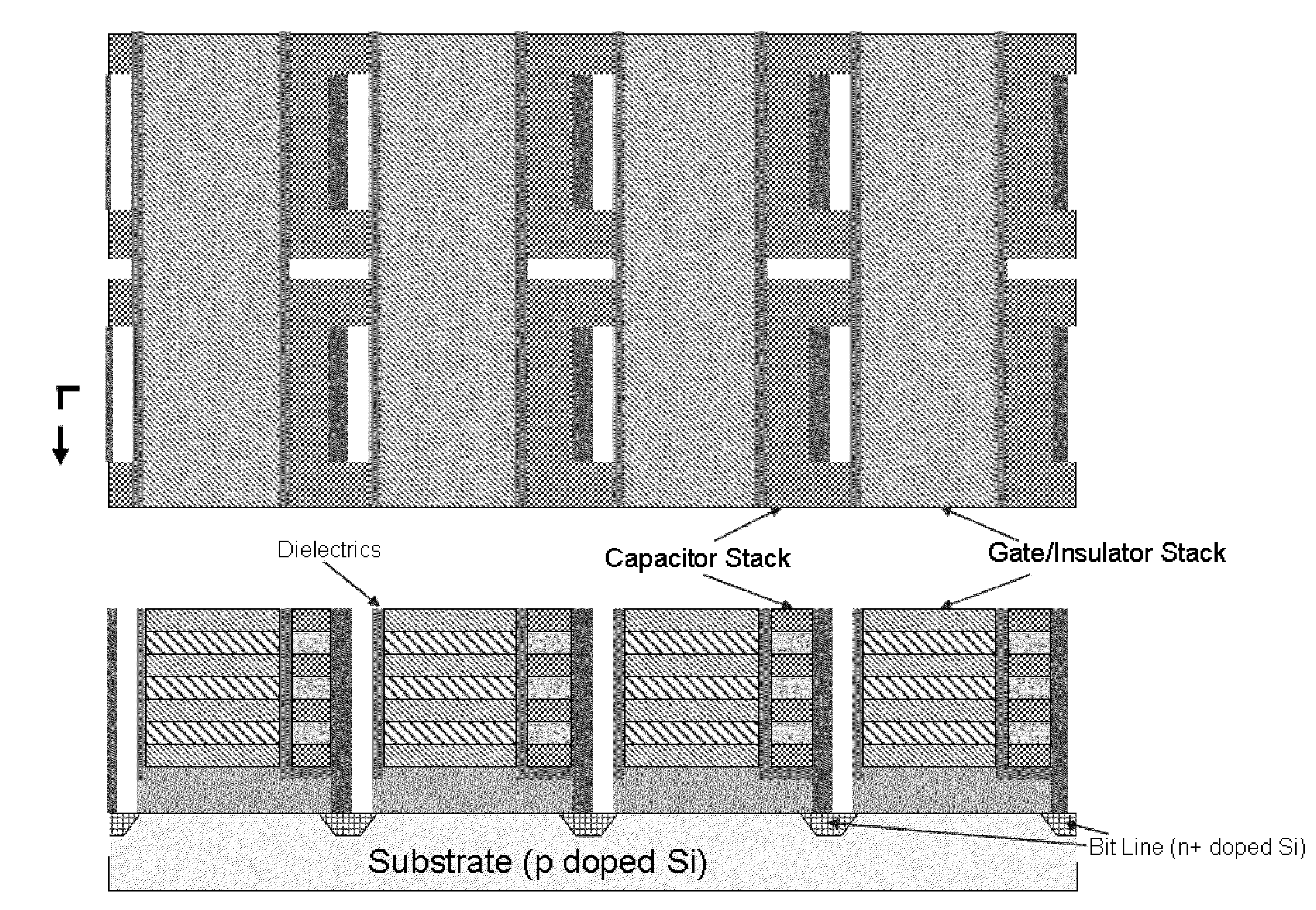
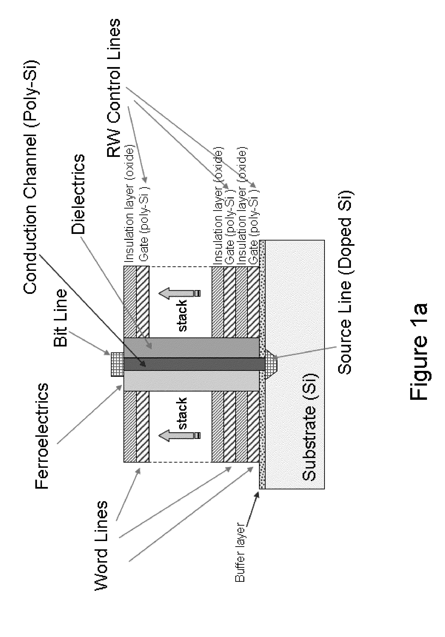
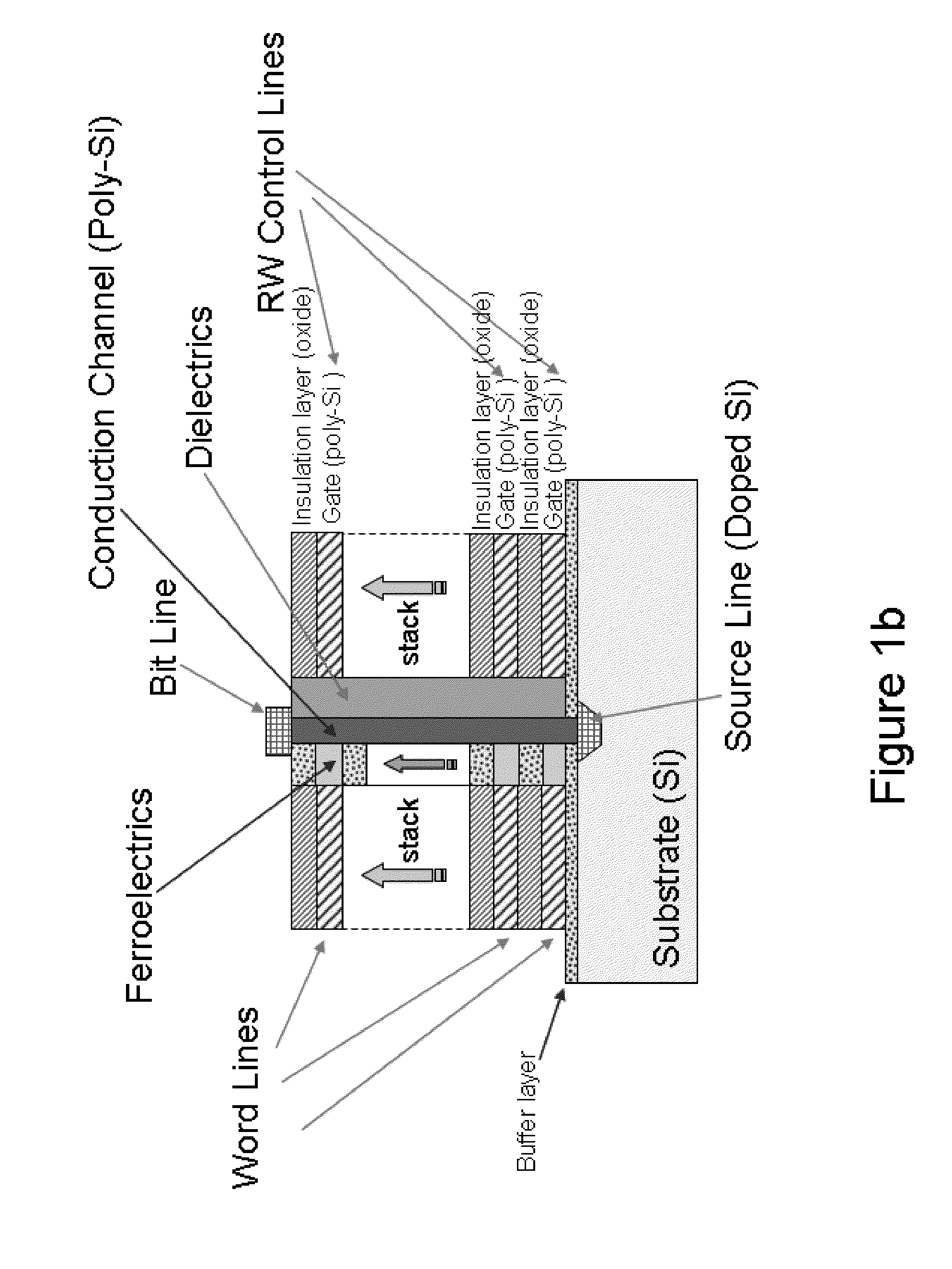
The present invention is related to the design of three-dimensional ferroelectric non-volatile memory devices with field-effect-transistors (FETs) electrically connected either in series or in parallel as a basic memory group to achieve high storage densities, as well as the design of double-gate structures for implementing read / write schemes to address every individual memory cells with full random access for such ferroelectric memory devices, with read schemes using OR-NAND or AND-NOR logics. The fabrication processes for such memory devices are also described.

Problems solved by technology

However, the storage density in currently available FeRAM is much lower than that of flash memories, making FeRAMs higher cost and thus commercially less competitive in most cases except for certain niche applications.

Method used


Image

  • Three-dimensional non-volatile ferroelectric random access memory
  • Three-dimensional non-volatile ferroelectric random access memory
  • Three-dimensional non-volatile ferroelectric random access memory

Examples


Embodiment Construction

[0021]The present invention provides a design of three-dimensional ferroelectric non-volatile memory devices for increasing the storage density. The key components are: 1) design of vertical and planar OR-NAND FeRAMs with FETs connected in series as a basic memory group and a read / write scheme with full random access to individual memory cells; 2) design of vertical and planar AND-NOR FeRAMs with FETs connected in parallel as a basic memory group and a read / write scheme with full random access to individual memory cells; 3) design of double-gate structure for implementing read / write schemes for the proposed OR-NAND FeRAMs and AND-NOR FeRAMs, where one type of gates (serving as the Word Line) employs ferroelectrics layers as gate dielectrics while the other type of gates (serving as the RW Control Line for read / write operations) employs conventional dielectric materials as gate dielectrics; (4) design of three-dimensional transistor-capacitor type NAND FeRAMs with stacked ferroelectr...


PUM


Abstract

The present invention provides a design of three-dimensional non-volatile ferroelectric random access memory (FeRAM) devices for increasing the storage density. The key components include: (1) FeRAM device structures with (i) field-effect-transistors electrically connected either in series or in parallel as a basic memory group and (ii) a double-gate structure for implementing read / write schemes with full random access to individual memory cells, where one type of gates employs ferroelectrics layers as the gate dielectrics while the other type of gates employs conventional dielectric materials as the gate dielectrics; and (2) FeRAM device structures with stacked ferroelectric-capacitors and field-effect-transistors electrically connected in series as a basic NAND memory group. Example fabrication processes for implementing such three-dimensional FeRAM devices are also provided.

Description

RELATED APPLICATIONS[0001]This application claims the benefit of and priority to (1) U.S. Provisional Patent Application No. 62 / 061,700, entitled “DESIGN OF THREE-DIMENSIONAL NON-VOLATILE FERROELECTRIC RANDOM ACCESS MEMORY,” filed Oct. 9, 2014; and (2) U.S. Provisional Patent Application No. 62 / 068,739, entitled “DESIGN OF THREE-DIMENSIONAL NON-VOLATILE FERROELECTRIC RANDOM ACCESS MEMORY,” filed Oct. 26, 2014; the entire content of which are hereby incorporated by reference for all purposes as if set forth herein.FIELD OF THE INVENTION[0002]The present invention relates to design of three-dimensional ferroelectric non-volatile memory devices for increasing the storage density. The key components are: 1) the design of stacked device structures for ferroelectric non-volatile memory; 2) the design of double-gate structures for implementing read / write schemes with full random access to individual memory cells, where one type of gates (serving as the Word Line) employs a ferroelectrics l...

Claims


Application Information

Patent Timeline
IPC IPC(8): H01L27/115H01L29/78H01L29/16H01L29/51
CPCH01L27/11597H01L27/1159H01L29/516H01L27/11514H01L29/517H01L29/16H01L27/11507H01L29/78391H10B53/10H10B53/20H10B51/10H10B51/20H10B51/30H10B53/30
Inventor PENG, HAIBING
Owner PENG HAIBING
Learn More