Pixel structure and driving method thereof

a technology of pixel structure and driving method, which is applied in the field of display technology and driving method, can solve the problems of corresponding decrease in the display quality, problems and disadvantages of existing products that require further improvement, and the skilled in the art have yet to find a solution, so as to improve the aperture ratio of pixels, maintain brightness and display quality, and improve the effect of improving the problem of transistor variability and aging

Inactive Publication Date: 2016-05-05
AU OPTRONICS CORP
View PDF6 Cites 46 Cited by
  • Summary
  • Abstract
  • Description
  • Claims
  • Application Information

AI Technical Summary

Benefits of technology

[0012]In view of the foregoing, embodiments of the present disclosure provide a pixel structure and a driving method to maintain brightness and display quality of a display by improving problems associated with transistor variability and aging of an AMOLED display, and to improve the problem of the aperture ratio of pixels decreasing due to the number of transistors in the pixel structure being high.

Problems solved by technology

However, problems of transistor variability and aging of the AMOLED display result in brightness unevenness, resulting in the display quality of the display being correspondingly decreased.
In view of the foregoing, problems and disadvantages are associated with existing products that require further improvement.
However, those skilled in the art have yet to find a solution.

Method used


Image

  • Pixel structure and driving method thereof
  • Pixel structure and driving method thereof
  • Pixel structure and driving method thereof

Examples


Embodiment Construction

[0042]The detailed description provided below in connection with the appended drawings is intended as a description of the present examples and is not intended to represent the only forms in which the present example may be constructed or utilized. The description sets forth the functions of the example and the sequence of steps for constructing and operating the example. However, the same or equivalent functions and sequences may be accomplished by different examples.

[0043]Unless otherwise defined herein, scientific and technical terminologies employed in the present disclosure shall have the meanings that are commonly understood and used by one of ordinary skill in the art. Unless otherwise required by context, it will be understood that singular terms shall include plural forms of the same and plural terms shall include singular forms of the same.

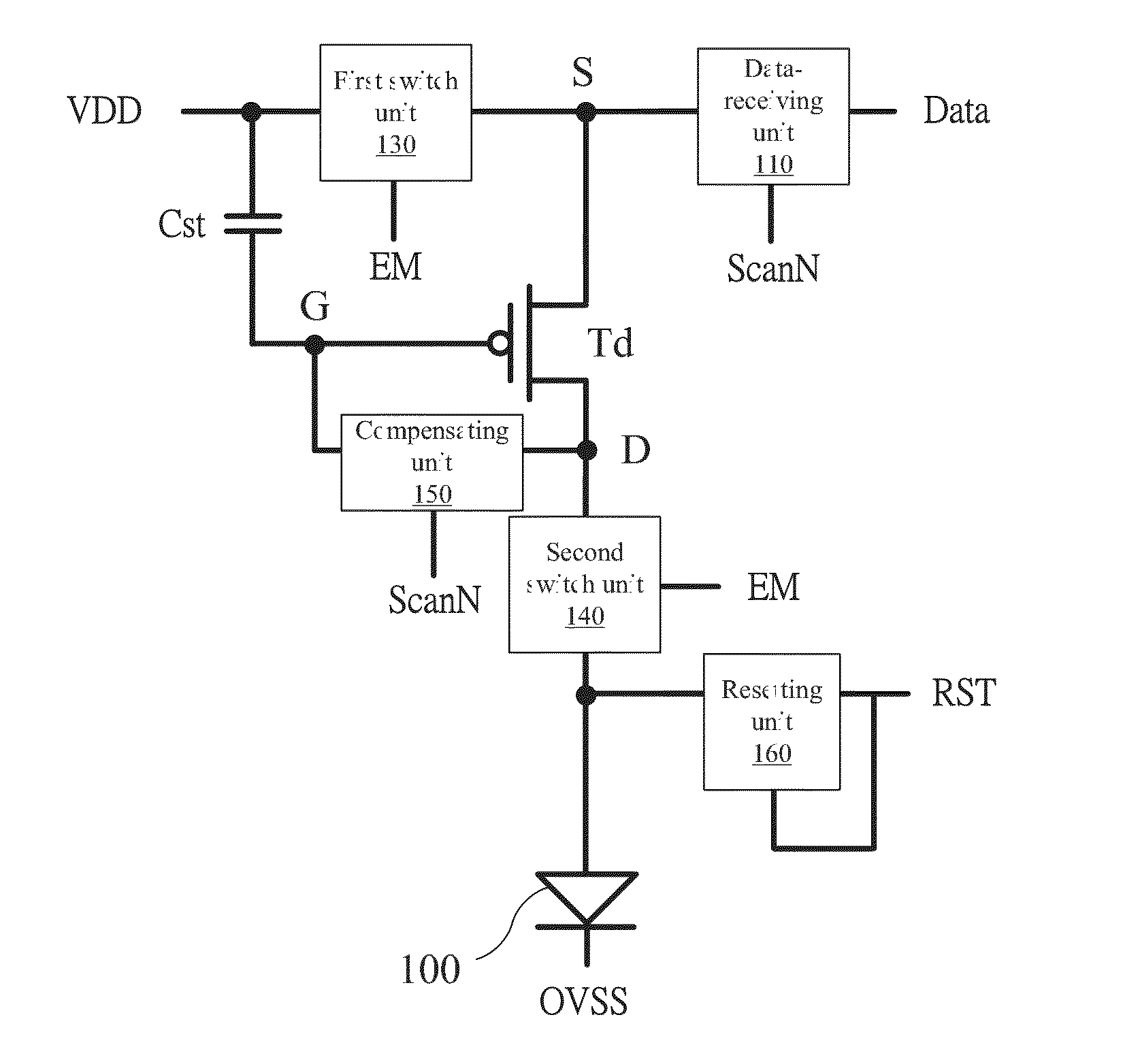
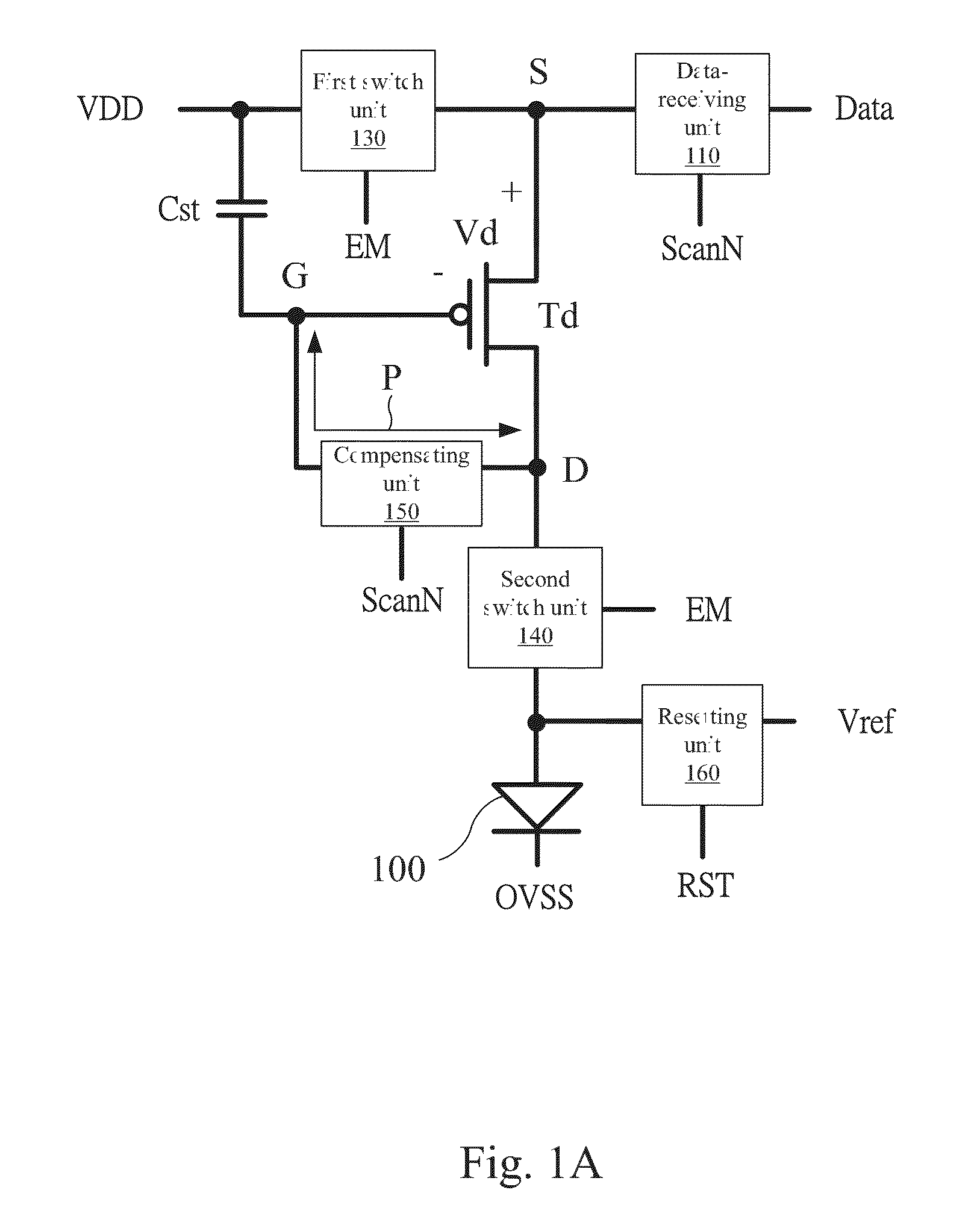
[0044]A 7T1C (seven transistors and one capacitors) configuration is used in the conventional pixel structure in order to compensate fo...


PUM


Abstract

A pixel structure includes a light-emitting diode, a transistor, a data-receiving unit, a compensating unit, and a resetting unit. The transistor is configured to be electrically coupled to the light-emitting diode, and drive the light-emitting diode based on a voltage difference between the control terminal and the first terminal of the transistor. The data-receiving unit is configured to be electrically coupled to the first terminal of the transistor, and provide a pixel date signal to the first terminal of the transistor based on a first scan signal. The compensating unit is electrically coupled to the control terminal and the second terminal of the transistor to act as a current path therebetween. The resetting unit is electrically coupled to the light-emitting diode. The resetting unit is configured to respectively provide a reverse bias and reference voltage to the light-emitting diode and the control terminal of the transistor.

Description

RELATED APPLICATIONS[0001]This application claims priority to Taiwan Application Serial Number 103137880, filed Oct. 31, 2014, which is herein incorporated by reference.BACKGROUND[0002]1. Field of Invention[0003]The present invention relates to display technology and a driving method. More particularly, the present invention relates to a pixel structure and a driving method.[0004]2. Description of Related Art[0005]With progress in technology, display technology has been continuously improving. An active-matrix organic light-emitting diode (AMOLED) display is presently one of the most important display technologies. Compared with the thin-film-transistor liquid-crystal display (TFT-LCD), display devices fabricated using AMOLED technology have a number of advantages, such as self-luminosity, wide viewing angle, high contrast, and fast response. Hence, AMOLED technology is widely applied in the displays of electronic devices.[0006]For driving an AMOLED display, pixel structures compose...

Claims


Application Information

Patent Timeline
Patent Type & Authority Applications(United States)
IPC IPC(8): G09G3/32G09G3/3258G09G3/3266
CPCG09G3/3258G09G3/3266G09G2330/028G09G2310/0202G09G2300/0809G09G3/3233G09G2300/0819G09G2320/045
Inventor HSU, WEI-CHUWU, PI-CHENGJEN, KO-RUEYLEE, CHIEN-YA
Owner AU OPTRONICS CORP
Why Eureka
Try Eureka