
Wireless Charging and Near Field Communication Dual Coils PCB Structure

a dual coil and pcb technology, applied in the direction of transformers, inductances, transportation and packaging, etc., can solve the problems of disadvantageous to the compact requirement of portable electronic devices, and the importance of near field communication (nfc), and achieve the effect of saving the space of the printed circuit board

Inactive Publication Date: 2016-05-05
TDK TAIWAN
View PDF6 Cites 89 Cited by
  • Summary
  • Abstract
  • Description
  • Claims
  • Application Information

AI Technical Summary

Benefits of technology

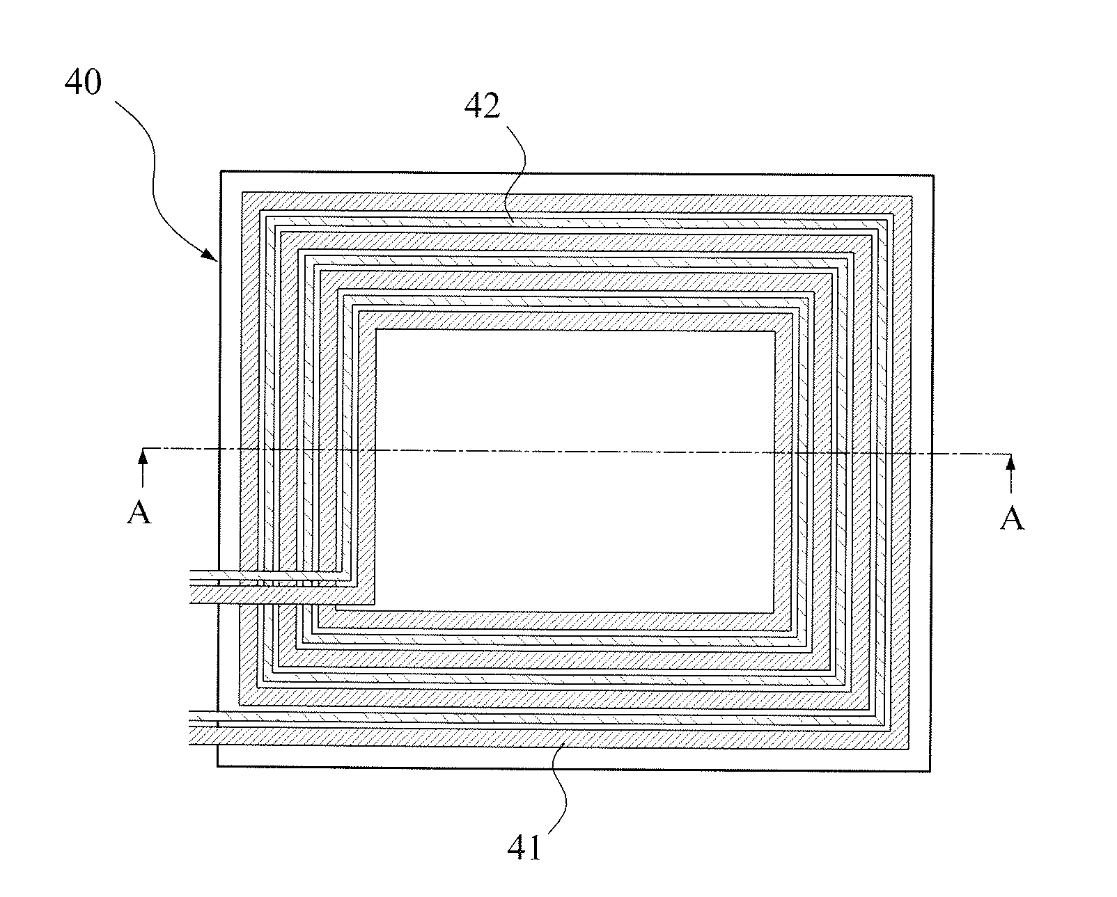
The present invention provides a way to save space on a printed circuit board by using a dual coil structure for wireless charging and near field communication. This allows for the NFC coil to be placed on the board without taking up space that could be used for the WLC coil. This arrangement still complies with industry standards, such as A4WP, which saves on space on the board.

Problems solved by technology

Moreover, near field communication (NFC) is also an important issue for portable electronic devices because NFC provides non-contact point-to-point communication for the portable electronic devices.
However, the circuit board mounting the WLC coil generally is area-restricted by certain standard, and the restricted area of the circuit board should be enlarged if NFC chip is to be mounted thereon.
This is in disadvantageous to the compact requirement of portable electronic devices.

Method used


Image

  • Wireless Charging and Near Field Communication Dual Coils PCB Structure
  • Wireless Charging and Near Field Communication Dual Coils PCB Structure
  • Wireless Charging and Near Field Communication Dual Coils PCB Structure

Examples


Embodiment Construction

[0021]Hereinafter, the embodiments of the present invention will be described with reference to the associated drawings. It should be noted various exemplary embodiments shown in the figures are merely illustrative representations and are not necessarily the limit of the claim scope.

[0022]With reference to FIGS. 3 and 4, FIG. 3 shows a schematic view of the WLC (A4WP) and NFC dual coils PCB structure according to an embodiment of the present invention, and FIG. 4 shows a sectional view along line A-A in FIG. 3. The embodiment shown in FIGS. 3 and 4 comprises a printed circuit board 40, which can be a single-faced circuit board. At least one WLC coil 41 complied with A4WP standard and at least one NFC coil 42 are arranged on a face of the printed circuit board 40. The printed circuit board 40 is arranged on a ferrite plate 50 such that the printed circuit board 40 can function as an induction-transmission plate for A4WP charging.

[0023]The coil wire of the WLC (A4WP) coil 41 is spiral...


PUM


Abstract

A wireless charging (WLC) (A4WP) and near field communication (NFC) dual coils PCB structure comprising at least one WLC (A4WP) coil wire having spiral shape and disposed on a printed circuit board (PCB), and a NFC coil wire having spiral shape and disposed on the PCB. At least a portion of the coil wire of the spiral WLC (A4WP) coil is located on a region between two adjacent coil wires of the spiral NFC coil. Therefore, the present invention makes use of spaces of WLC (A4WP) coil such as A4WP or other relevant standards combined with the NFC coil, so that the dual coil of the present invention can reduce the area of the PCB occupied by the electronic device.

Description

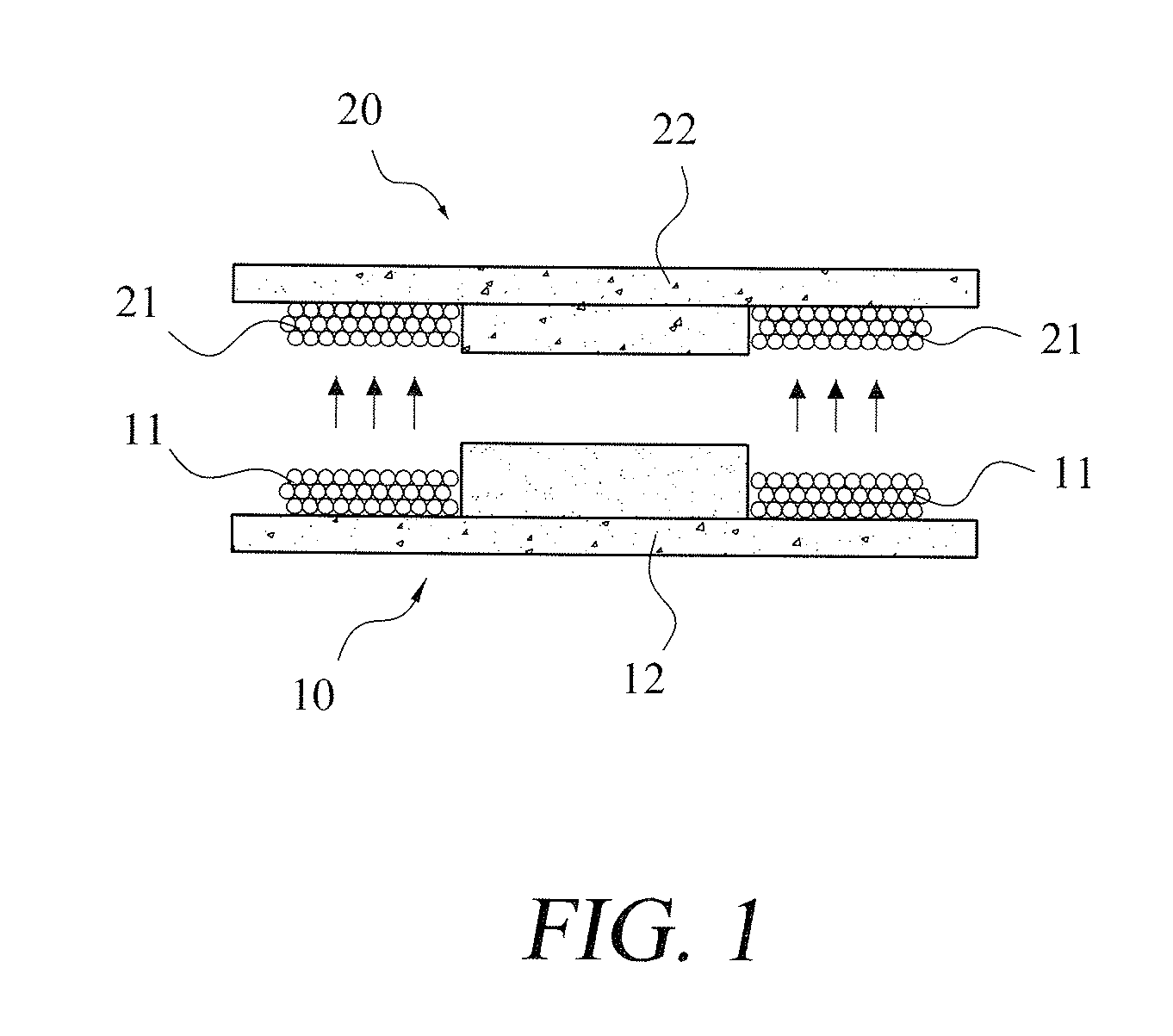
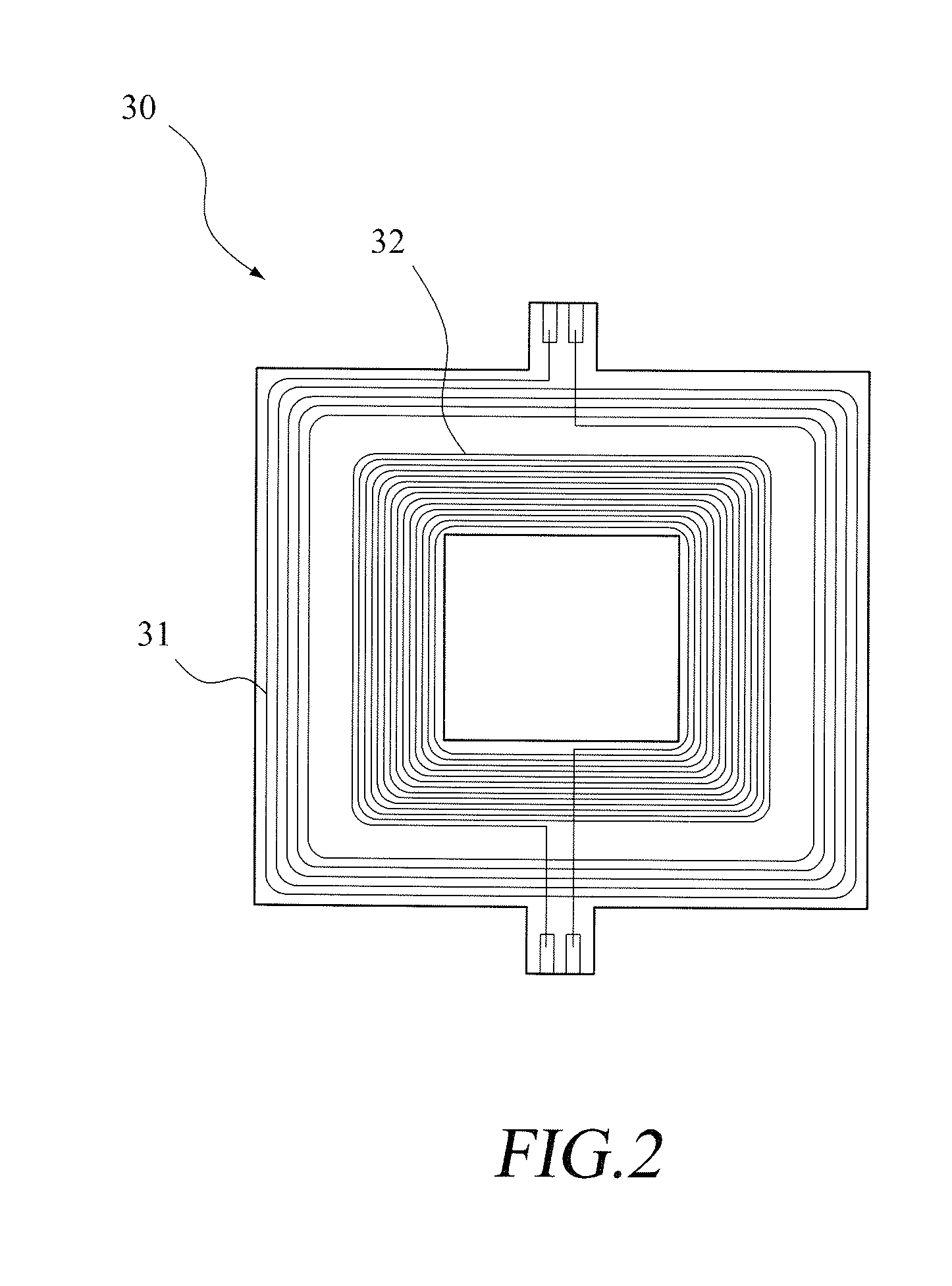
BACKGROUND OF THE INVENTION[0001]1. Field of the Invention[0002]The present invention relates to a dual coils PCB structure, especially to a wireless charging (WLC) A4WP and near field communication (NFC) dual coils PCB structure.[0003]2. Description of the Prior Art[0004]The portable electronic devices, such as PDAs, palm computers, laptop computers or tablet computers, generally use rechargeable battery as power source, so user can still use the portable electronic devices when wall socket power is not available. The portable electronic devices are also equipped with wired power supply to charge the rechargeable battery or power the portable electronic devices with wall socket power.[0005]The rechargeable battery in the portable electronic devices can be charged with electromagnetic induction (such as A4WP wireless charging techniques); therefore a physical power line can be dispensed with. FIG. 1 is a schematic diagram showing the wireless charging scheme. The shown wireless char...

Claims


Application Information

Patent Timeline
IPC IPC(8): H01F27/28H01F38/14H01F27/29H02J7/02
CPCH01F27/2804H02J7/025H01F2027/2809H01F27/29H01F38/14H02J7/0042H02J50/20H02J50/80H04B5/00H02J50/005H02J50/70H01F27/36H01F27/366H04B5/72H04B5/79H04B5/26H04B5/43
Inventor CHIEN, FENG-LUNGOISHI, TAKAHIROCHEN, MAO-CHUNWU, CHI-FUCHANG, CHAO-NEEN
Owner TDK TAIWAN
Learn More