Method of fabricating a tungsten plug in a semiconductor device
a technology of semiconductor devices and tungsten plugs, which is applied in the direction of semiconductor devices, semiconductor/solid-state device details, electrical equipment, etc., can solve the problems of natural tungsten seam formation, enlargement or enhancement of seams,
- Summary
- Abstract
- Description
- Claims
- Application Information
AI Technical Summary
Benefits of technology
Problems solved by technology
Method used
Image

Examples
Embodiment Construction
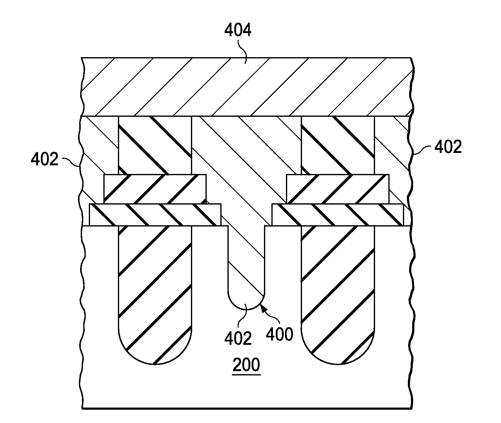
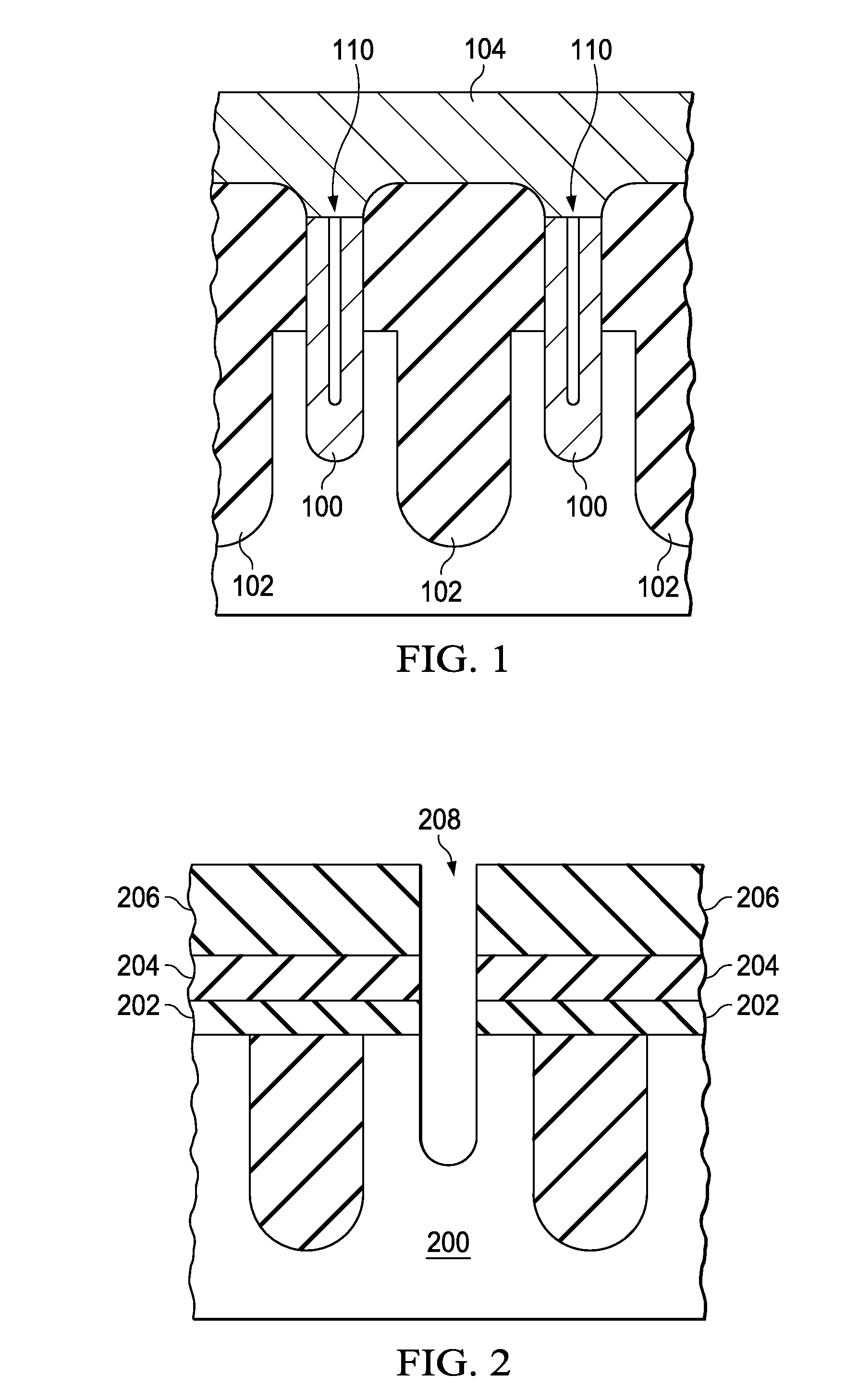
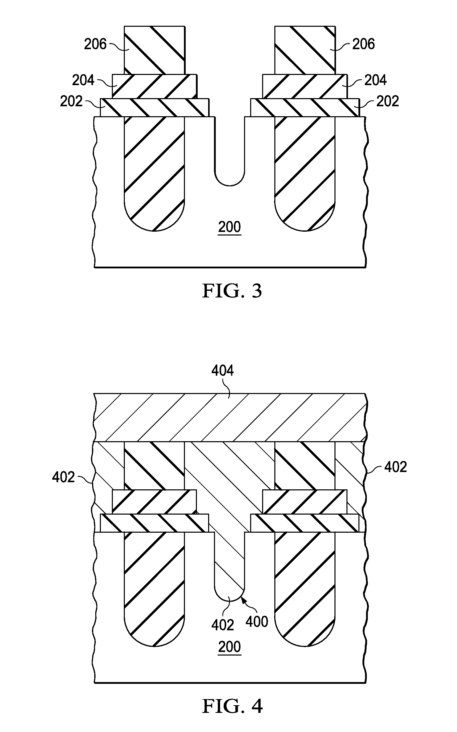
[0013]One embodiment of the present invention is shown in FIGS. 2-4. In order to address the tungsten plug seam problem, the interlayer dielectric is composed of multiple layers of dielectric material with different wet etch rates. In this embodiment three different oxide layers are formed on the silicon substrate 200. First a thermal oxide layer 202 is formed using a high temperature oxidizing agent such as water vapor or molecular oxygen to diffuse into the silicon substrate and react to form a thin SiO2 layer 202. The thermal oxide or SiO2 layer 202 may be between 100 and 700 Angstroms thick. A Tetraethylorthosilicate (TEOS) oxide layer 204 is subsequently formed by chemical vapor deposition (CVD), or can be a furnace grown TEOS, on top of the thermal oxide layer 202, followed by a Borophosphosilicate Glass (BPSG) layer 206. The TEOS layer may be between 800 and 1600 Angstroms thick, while the BPSG layer may be between 2500 and 4500 Angstroms thick.
[0014]In the present embodiment...
PUM
| Property | Measurement | Unit |
|---|---|---|
| thick | aaaaa | aaaaa |
| thick | aaaaa | aaaaa |
| thick | aaaaa | aaaaa |
Abstract
Description
Claims
Application Information