
Eureka
For R&D, Eureka makes reading and utilizing patents & technical documents easy.
Eureka AIR
Designed for self-driven R&D workflows. Generate viable solutions, solve complex R&D challenges, empower your innovation with AI.

Eureka Materials
Designed for material experts only. Revolutionize your material R&D, from search, analyze, to developing new materials.

TechResearch
Generate reliable direction feasibility study reports for your R&D in just a few steps.

TechSeek
Discover and master advanced knowledge NOW. Basics, ideas, possibilities, all at once.

TechMind
As an expert in R&D Theories, TechMind can generates customized viable solutions instantly.

TechRisk
Analyze your overall solution with one click, know your potential R&D risks in advance.

TechMonitor
Get weekly tech updates, stay abreast of the latest tech innovations and key insights.
Vertical hall element
- Summary
- Abstract
- Description
- Claims
- Application Information
AI Technical Summary
Benefits of technology
Problems solved by technology
Method used
Image

Examples
first embodiment
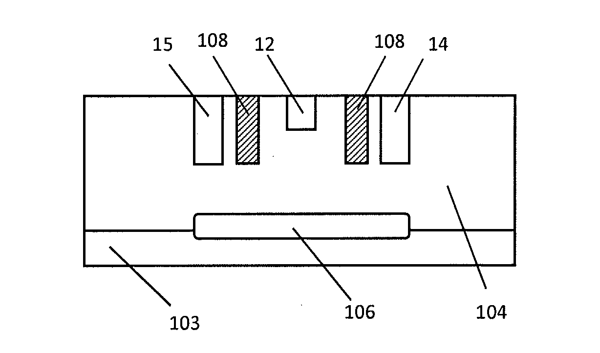
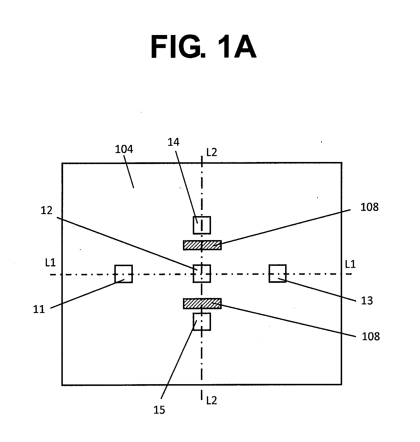
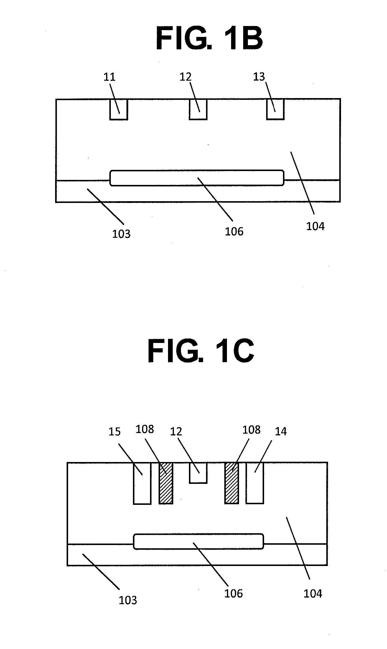
[0051]FIG. 1A to FIG. 1C are schematic views for illustrating a vertical Hall element according to a first embodiment of the present invention. FIG. 1A is a plan view, FIG. 1B is a sectional view taken along the line L1-L1 of FIG. 1A, and FIG. 1C is a sectional view taken along the line L2-L2 of FIG. 1A.
[0052]An epitaxial layer 104 that is an n-type semiconductor layer serving as a magnetic sensing portion is formed on a p-type semiconductor substrate 103. An n-type impurity layer (buried layer) 106 having an impurity concentration higher than that of the epitaxial layer 104 is formed at the bottom of the epitaxial layer 104 in contact with the p-type semiconductor substrate 103. Current supply ends 11 to 13 for supplying Hall current and voltage output ends 14 and 15 for detecting Hall voltage are heavily doped n-type impurity layers, and are arranged from a surface of the epitaxial layer 104 to inside of the epitaxial layer 104. The buried layer 106 is formed beneath the regions o...
second embodiment
[0058]FIG. 2A to FIG. 2C are schematic views for illustrating a vertical Hall element according to a second embodiment of the present invention. FIG. 2A is a plan view, FIG. 2B is a sectional view taken along the line L1-L1 of FIG. 2A, and FIG. 2C is a sectional view taken along the line L2-L2 of FIG. 2A.
[0059]The second embodiment is different from the first embodiment in the shape of the trenches 108 formed between the voltage output ends 14 and 15 and the current supply end 12, respectively, and the rest of the structure is the same as that of the first embodiment. With reference to FIG. 2A, the trenches 108 are shaped so as to surround the voltage output ends 14 and 15, respectively, in plan view. This can restrict a flow of current into the voltage output ends 14 and 15 with more reliability to enhance the sensitivity. In FIG. 2A, the trenches 108 are shaped so as to completely surround the voltage output ends 14 and 15, respectively, but the trenches 108 may be shaped so as to...
third embodiment
[0062]FIG. 3A to FIG. 3C are schematic views for illustrating a vertical Hall element according to a third embodiment of the present invention. FIG. 3A is a plan view, FIG. 3B is a sectional view taken along the line L1-L1 of FIG. 3A, and FIG. 3C is a sectional view taken along the line L2-L2 of FIG. 3A.
[0063]This embodiment is different from the first embodiment in a diffused separating wall 107 that is a heavily doped p-type impurity region formed so as to separate the three current supply ends 11 to 13 from one another, and the rest of the structure is the same as that of the first embodiment. The p-type diffused separating wall 107 is formed so as to surround the current supply end 11 and to surround the current supply end 13, and further, to surround the current supply end 12, the voltage output ends 14 and 15, and the trenches 108. As a result, the diffused separating wall 107 is a diffused region having three windows that have no p-type impurity diffused therein. The p-type d...
PUM
 Abstract
Description
Claims
Application Information
 - R&D Engineer
- R&D Manager
- IP Professional
- Industry Leading Data Capabilities
- Powerful AI technology
- Patent DNA Extraction
Browse by: Latest US Patents, China's latest patents, Technical Efficacy Thesaurus, Application Domain, Technology Topic, Popular Technical Reports.
© 2024 PatSnap. All rights reserved.Legal|Privacy policy|Modern Slavery Act Transparency Statement|Sitemap|About US| Contact US: help@patsnap.com