Low voltage differential signaling (LVDS) driving circuit

a driving circuit and low voltage technology, applied in logic circuit coupling/interface arrangement, logic circuit coupling/interface using field-effect transistors, pulse techniques, etc., can solve the problems of insufficient head room of current sources and very limited output range of differential signaling circuits

Active Publication Date: 2016-05-26
VIA ALLIANCE SEMICON CO LTD
View PDF0 Cites 7 Cited by
  • Summary
  • Abstract
  • Description
  • Claims
  • Application Information

AI Technical Summary

Benefits of technology

[0071]The invention provides a novel design of LVDS driving circuit. In conclusion, the proposed LVDS driving circuit has at least the following advantages compared with the prior art: (1) omitting the use of current sources and current sinks; (2) increasing the head room and widening the output range; (3) being suitable for applications of advanced processes with very low supply voltages; (4) enhancing the operating speed; (5) decreasing the manufacturing cost, and (6) enhanced signal quality for high data transmission rates.

Problems solved by technology

However, conventional differential signaling circuits require bias currents which are driven by current sources.
As a result, the current sources may have insufficient head room, and the output range of the differential signaling circuits may be very limited.

Method used


Image

  • Low voltage differential signaling (LVDS) driving circuit
  • Low voltage differential signaling (LVDS) driving circuit
  • Low voltage differential signaling (LVDS) driving circuit

Examples


Embodiment Construction

[0049]In order to illustrate the purposes, features and advantages of the invention, the embodiments and figures of the invention are described in detail as follows.

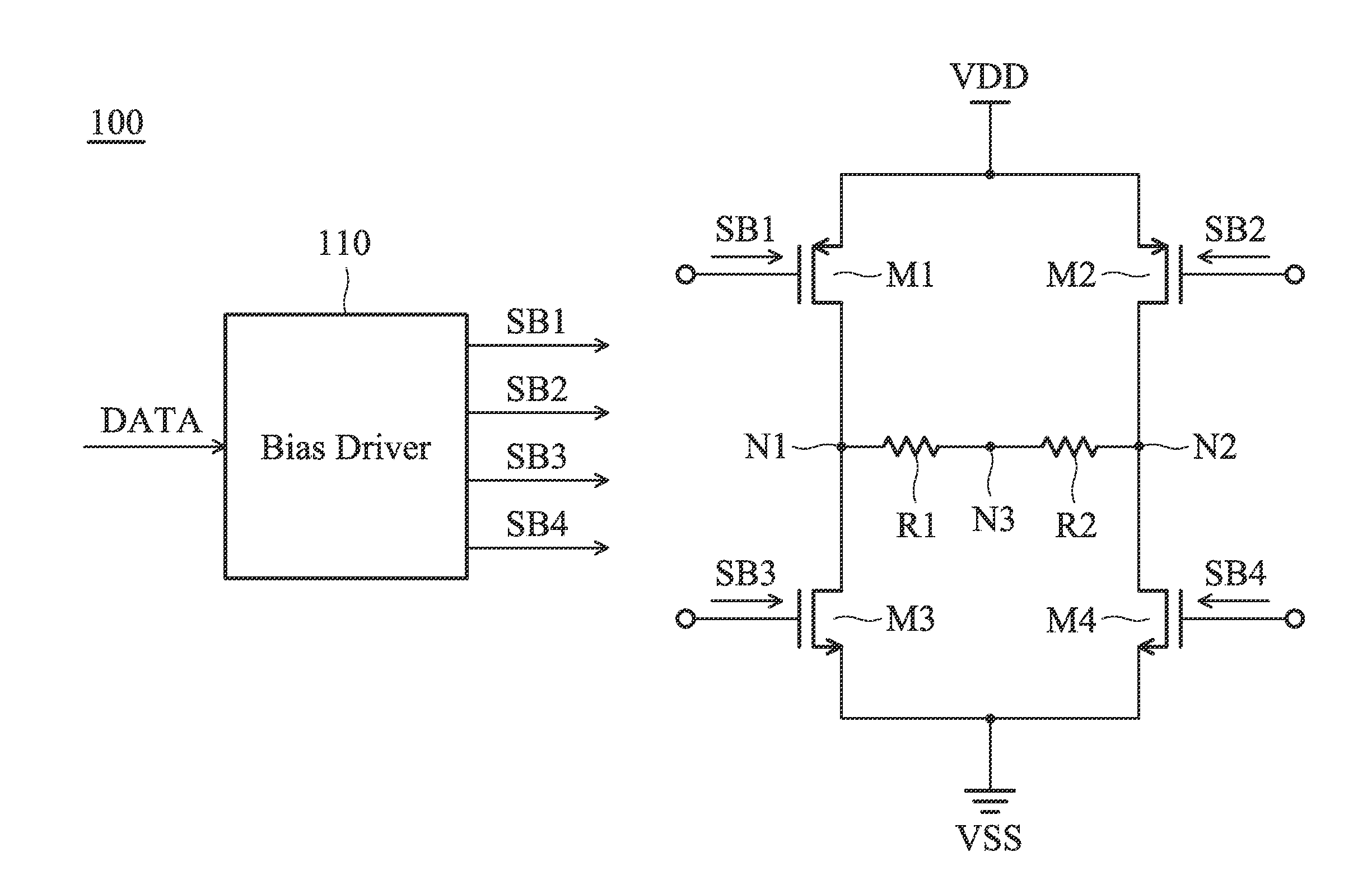
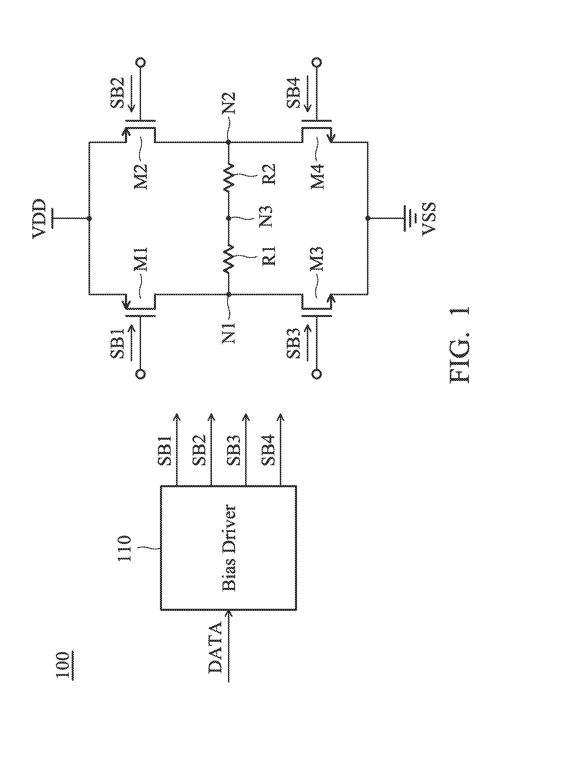
[0050]FIG. 1 is a diagram of an LVDS (Low Voltage Differential Signaling) driving circuit 100 according to an embodiment of the invention. The LVDS driving circuit 100 includes a first transistor M1, a second transistor M2, a third transistor M3, a fourth transistor M4, a first resistor R1, a second resistor R2, and a bias driver 110. The bias driver 110 generates a first bias signal SB1, a second bias signal SB2, a third bias signal SB3, and a fourth bias signal SB4 for controlling the first transistor M1, the second transistor M2, the third transistor M3, and the fourth transistor M4, respectively, according to a data signal DATA. The data signal DATA may be a digital signal. In some embodiments, the first transistor M1 and the second transistor M2 are PMOS transistors (P-type Metal Oxide Semiconductor Field Effect Tra...


PUM


Abstract

An LVDS (Low Voltage Differential Signaling) driving circuit includes a first transistor, a second transistor, a third transistor, a fourth transistor, a first resistor, a second resistor, and a bias driver. The first transistor is coupled between a supply voltage and a first node. The second transistor is coupled between the supply voltage and a second node. The third transistor is coupled between the first node and a ground voltage. The fourth transistor is coupled between the second node and the ground voltage. The first resistor is coupled between the first node and a third node. The second resistor is coupled between the second node and the third node. The bias driver generates bias signals for controlling the first, second, third, and fourth transistors according to a data signal.

Description

CROSS REFERENCE TO RELATED APPLICATIONS[0001]This application is a Continuation-In-Part of application Ser. No. 14 / 551,280, filed on Nov. 24, 2014, the entirety of which is incorporated by reference herein.BACKGROUND OF THE INVENTION[0002]1. Field of the Invention[0003]The disclosure generally relates to an LVDS (Low Voltage Differential Signaling) driving circuit, and more particularly, to an LVDS driving circuit with a simplified circuit structure and a high operating speed.[0004]2. Description of the Related Art[0005]Differential signaling circuits are very popular, being used in data transmission nowadays, including LVDS (Low Voltage Differential Signaling), HDMI (High-Definition Multimedia Interface), and USB (Universal Serial Bus), etc. Differential signaling circuits have power saving and noise rejection advantages. However, conventional differential signaling circuits require bias currents which are driven by current sources. With the progress in manufacturing technology, th...

Claims


Application Information

Patent Timeline
Patent Type & Authority Applications(United States)
IPC IPC(8): H03K19/0185H03K19/21
CPCH03K19/018528H04L25/0272H03K19/018514H03K19/21
Inventor LEE, YEONG-SHENG
Owner VIA ALLIANCE SEMICON CO LTD
Why Eureka
Try Eureka