Liquid crystal display device and method of manufacturing the same

a technology of liquid crystal display and liquid crystal, which is applied in the direction of optics, instruments, photomechanical equipment, etc., can solve the problems of high cost, long process time, heavy display device, etc., and achieve the effect of improving the removal characteristics, uniform display quality, and weigh

Inactive Publication Date: 2016-06-02
SAMSUNG DISPLAY CO LTD
View PDF1 Cites 0 Cited by
  • Summary
  • Abstract
  • Description
  • Claims
  • Application Information

AI Technical Summary

Benefits of technology

[0010]A liquid crystal display device having advantages of decreasing a weight, a thickness, a cost, and a process time by using a single substrate, and a method of manufacturing the same are provided.
[0011]In addition, a liquid crystal display device having a uniform and constant liquid crystal injection cavity through a negative photo resist having heat resistance and improved residue removal characteristics are provided.
[0027]According to an exemplary embodiment, in the liquid crystal display device and the method of manufacturing the same as described above, the display device is manufactured using a single substrate, such that a weight, a thickness, a cost, and a process time may be decreased.
[0028]In addition, a uniform and constant liquid crystal injection cavity through a negative photo resist having heat resistance and improved residue removal characteristics may be provided. Therefore, a display device having uniform display quality may be provided.

Problems solved by technology

However, because two substrates are essentially used in the liquid crystal display device according to the related art, and each constituent component is formed on the two substrates, there are problems in that the display device is heavy, thick, and expensive, and a process time is long, etc.

Method used


Image

  • Liquid crystal display device and method of manufacturing the same
  • Liquid crystal display device and method of manufacturing the same
  • Liquid crystal display device and method of manufacturing the same

Examples


Embodiment Construction

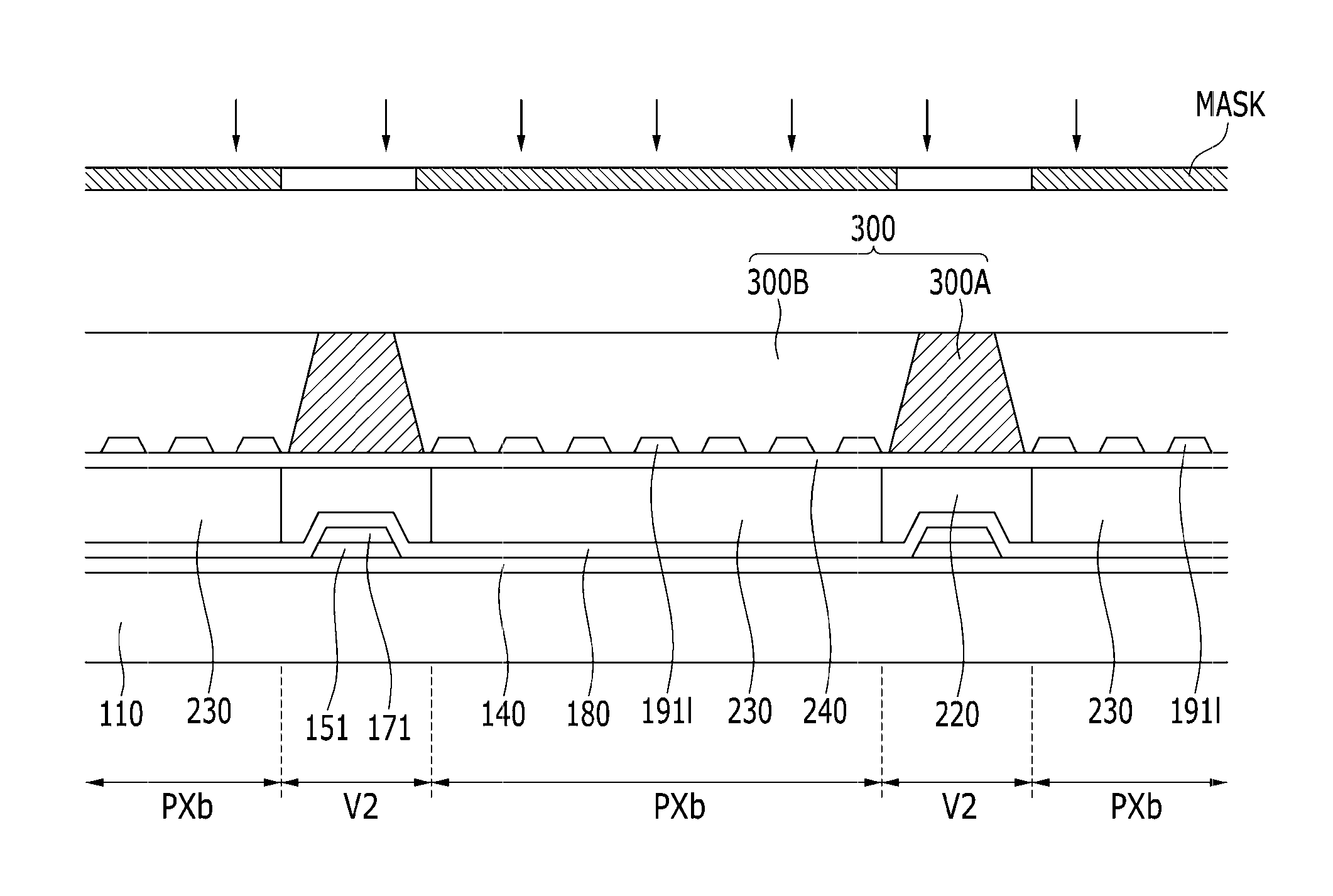
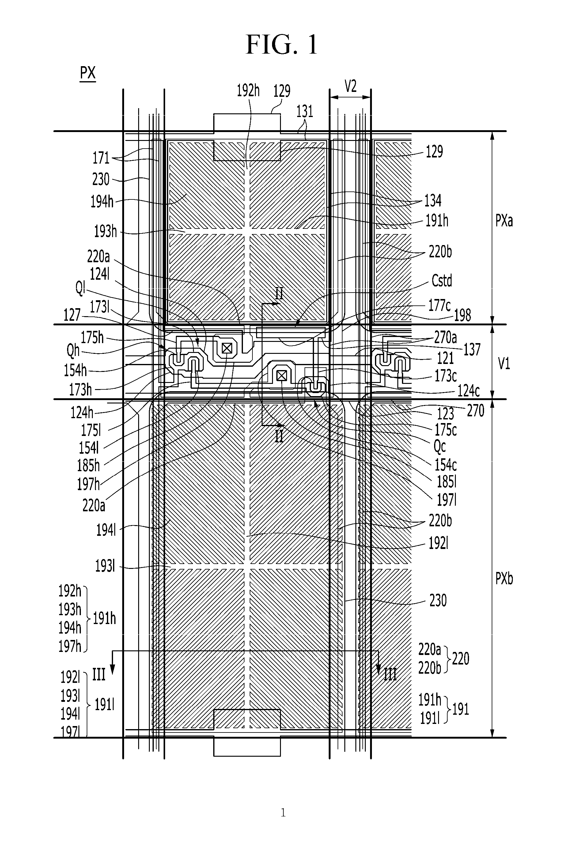
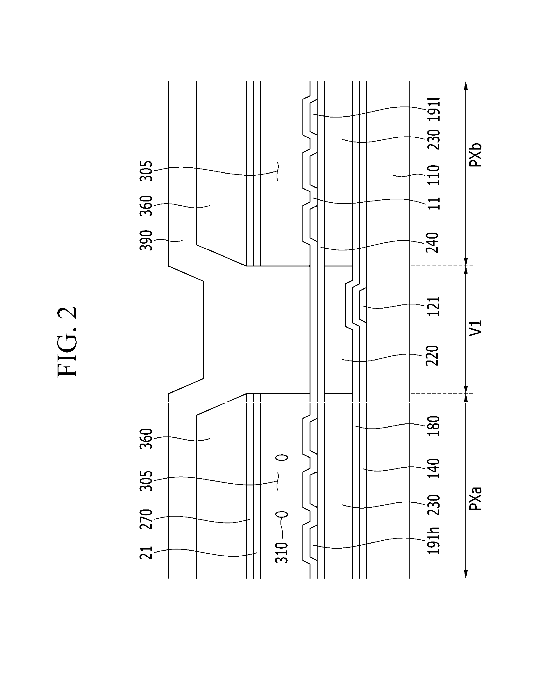
[0033]The present disclosure will be described more fully hereinafter with reference to the accompanying drawings, in which exemplary embodiments are shown. As those skilled in the art would realize, the described embodiments may be modified in various different ways, all without departing from the spirit or scope of the present disclosure.

[0034]In the drawings, the thicknesses of layers, films, panels, regions, etc., are exaggerated for clarity. Like reference numerals designate like elements throughout the specification. It will be understood that when an element such as a layer, film, region, or substrate is referred to as being “on” another element, it can be directly on the other element or intervening elements may also be present. In contrast, when an element is referred to as being “directly on” another element, there are no intervening elements present.

[0035]Hereinafter, a liquid crystal display device according to an exemplary embodiment will be described with reference to ...


PUM

PropertyMeasurementUnit
angleaaaaaaaaaa
angleaaaaaaaaaa
Chemical Formulaaaaaaaaaaa

Abstract

A liquid crystal display device includes: an insulating substrate, a thin film transistor positioned on the insulating substrate, a pixel electrode connected to the thin film transistor, a pillar portion positioned on the pixel electrode, a common electrode positioned on the pillar portion, a liquid crystal layer filling in a cavity positioned between the pixel electrode, the pillar portion, and the common electrode and containing liquid crystal molecules, and a roof layer and an overcoat positioned on the common electrode, wherein a cross section of the cavity in a column direction is reversely tapered.

Description

CROSS-REFERENCE TO RELATED APPLICATION[0001]This application claims priority to and the benefit of Korean Patent Application No. 10-2014-0168659 filed in the Korean Intellectual Property Office on Nov. 28, 2014, the entire contents of which are incorporated herein by reference.BACKGROUND[0002](a) Field[0003]The present invention relates to a liquid crystal display device and a method of manufacturing the same.[0004](b) Description of the Related Art[0005]A display device is required in computer monitors, televisions, mobile phones, and the like, which are widely used at this time. As the display device, there are a cathode ray tube display device, a liquid crystal display device, a plasma display device, and the like.[0006]The liquid crystal display device, which is one of flat panel display devices most widely used at present, is composed of two display panels in which electric field generating electrodes, such as a pixel electrode and a common electrode, are formed and a liquid cr...

Claims


Application Information

Patent Timeline
Patent Type & Authority Applications(United States)
IPC IPC(8): G02F1/1362G02F1/1339G02F1/1368
CPCG02F1/136209G02F1/13394G02F1/1368G02F1/136286G02F2001/136222G02F1/1303G02F1/1341G02F1/1362G03F7/004G02F1/136222G02F1/133377G02F1/13398G02F1/1339G02F1/1343Y10S359/90
Inventor JUNG, YANG HOKANG, HOONPARK, CHUL WONSUGITANI, KOICHIJU, JIN HO
Owner SAMSUNG DISPLAY CO LTD
Why Eureka
Try Eureka