Rc-stacked mosfet circuit for high voltage (HV) electrostatic discharge (ESD) protection

Active Publication Date: 2016-06-02
GLOBALFOUNDRIES SINGAPORE PTE LTD
View PDF5 Cites 13 Cited by
  • Summary
  • Abstract
  • Description
  • Claims
  • Application Information

AI Technical Summary

Benefits of technology

[0005]Embodiments generally relate to device and method of forming an integrated circuit (IC) that offers protection against ESD in high voltage (HV) circuit applications are disclosed. A device includes N ones of a field effect transistor (FET) stacked in series to provide an N-level stack, where N is an integer greater than 1. A first pad of the device is coupled to a fi

Problems solved by technology

Parasitic conductance in the N ones of the FET is triggered by the ESD event, the parasit

Method used


Image

  • Rc-stacked mosfet circuit for high voltage (HV) electrostatic discharge (ESD) protection
  • Rc-stacked mosfet circuit for high voltage (HV) electrostatic discharge (ESD) protection
  • Rc-stacked mosfet circuit for high voltage (HV) electrostatic discharge (ESD) protection

Examples


Embodiment Construction

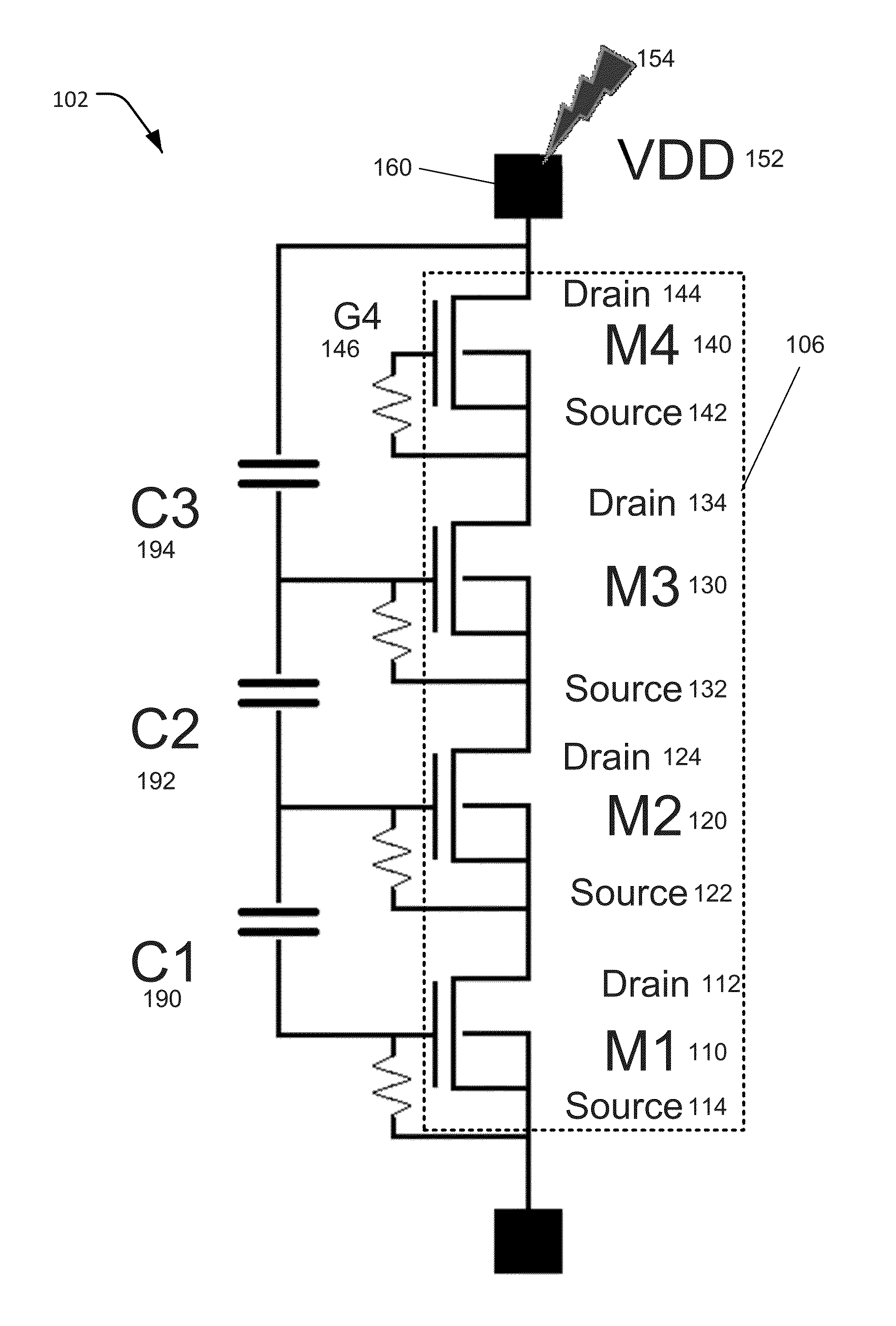
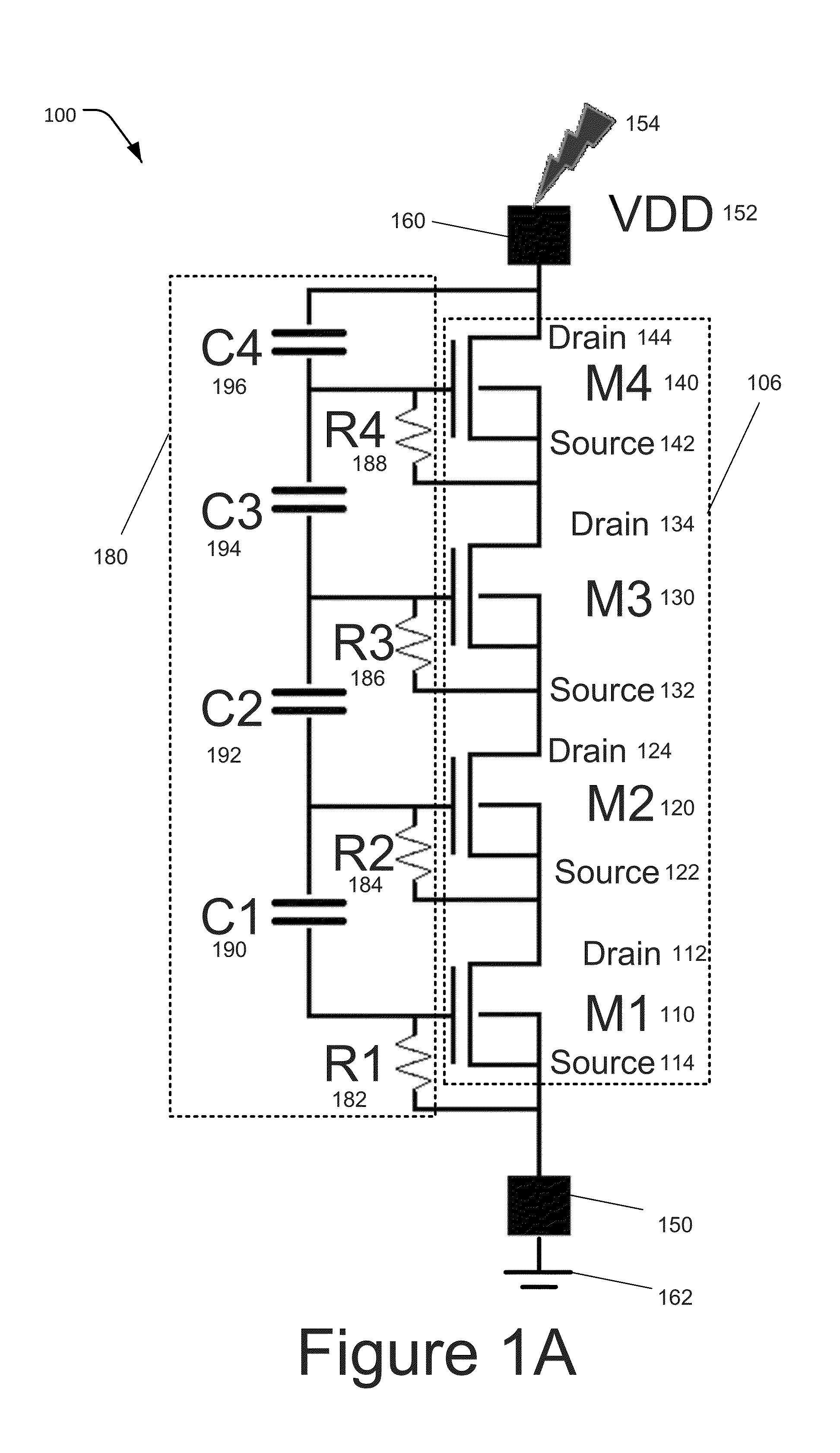
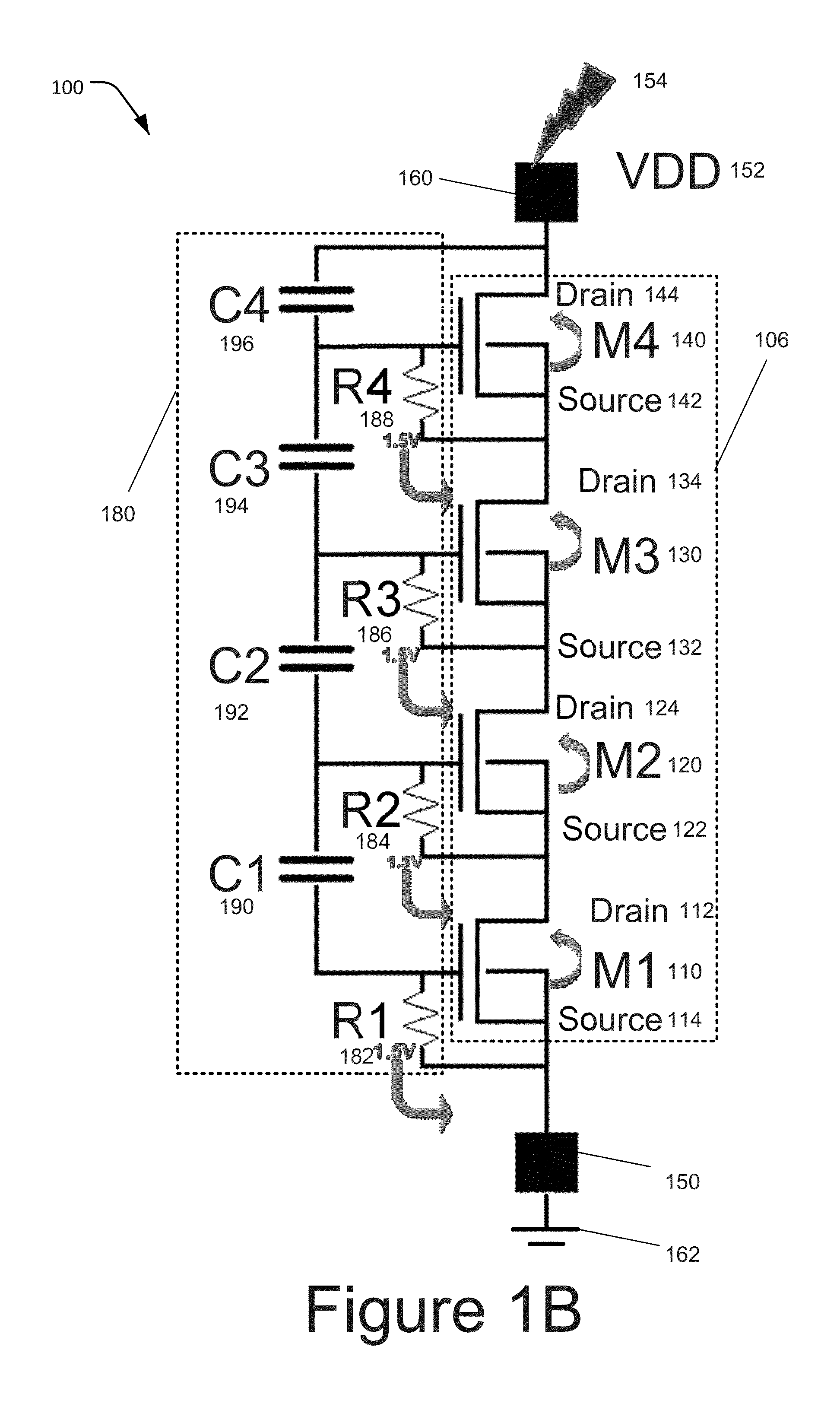
[0024]Novel features believed characteristic of the present disclosure are set forth in the appended claims. The disclosure itself, however, as well as a preferred mode of use, various objectives and advantages thereof, will best be understood by reference to the following detailed description of an illustrative embodiment when read in conjunction with the accompanying drawings. The functionality of various circuits, devices or components described herein may be implemented as hardware (including discrete components, integrated circuits and systems-on-a-chip ‘SoC’), firmware (including application specific integrated circuits and programmable chips) and / or software or a combination thereof, depending on the application requirements.

[0025]Similarly, the functionality of various mechanical elements, members, and / or components for forming modules, sub-assemblies and assemblies assembled in accordance with a structure for an apparatus may be implemented using various materials and coupl...


PUM


Abstract

Devices and methods of forming an integrated circuit (IC) that offer protection against ESD in high voltage (HV) circuit applications are disclosed. A device includes N ones of a field effect transistor (FET) stacked in series to provide an N-level stack, where N is an integer greater than 1. A first pad of the device is coupled to a first FET and a second pad is coupled to an Nth FET. The device also includes a stacked/distributed RC control circuit configured to cause a short circuit between the first pad and the second pad in response to an ESD event. During the ESD event, the RC control circuit is configured to concurrently provide sufficient voltage to control the N ones of the FET by turning them on using parasitic conduction to cause the short circuit.

Description

CROSS-REFERENCE TO RELATED APPLICATION[0001]This Application claims the benefit of and priority to U.S. Provisional Patent Application No. 62 / 085,630, filed Nov. 30, 2014, which is hereby incorporated by reference in its entirety.BACKGROUND[0002]High voltage (HV) integrated circuits used in power management, power conversion, LCD / display, automotive and other applications typically operate between 52 V and 100 V. Stacked field effect transistor (FET) based cell structures are often used in the design of HV circuits. An occurrence of an electrostatic discharge (ESD) can severely and irreparably damage unprotected electronic circuits, including HV integrated circuits. As such, many HV integrated circuit chips may include a built-in ESD device to pro vide some measure of protection against the undesirable flow of damage-causing currents.[0003]An ESD protection device in HV applications is typically prone to latch up errors since the FET operating voltages may exceed its design window (...

Claims


Application Information

Patent Timeline
IPC IPC(8): H01L27/02H01L27/06H01L49/02H01L21/762H01L21/8234H01L21/768H02H9/04H01L29/10
CPCH01L27/0277H02H9/04H01L27/0629H01L29/1095H01L28/40H01L21/823475H01L21/768H01L28/20H01L21/76224H01L21/77H01L27/0288H01L27/0274
Inventor LINEWIH, HANDOKOLI, MINGMARIMUTHU, SEVASHANMUGAMYU, RONGHUA
Owner GLOBALFOUNDRIES SINGAPORE PTE LTD
Why Eureka
Try Eureka