Thin-film solar cell and production method for thin-film solar cell

Active Publication Date: 2016-06-02
SOLAR FRONTIER
View PDF2 Cites 1 Cited by
  • Summary
  • Abstract
  • Description
  • Claims
  • Application Information

AI Technical Summary

Benefits of technology

The present patent text is about a method to produce a thin-film solar cell that has improved photoelectric conversion efficiency. This means that the cell can capture and convert more sunlight into electrical energy. This method can be used to produce thin-film solar cells that have better performance and can improve the overall efficiency of solar cells.

Problems solved by technology

It has been reported that Ga causes defects in the p-type light absorption layer and this leads to a reduction in the photoelectric conversion efficiency.

Method used


Image

  • Thin-film solar cell and production method for thin-film solar cell
  • Thin-film solar cell and production method for thin-film solar cell
  • Thin-film solar cell and production method for thin-film solar cell

Examples


Embodiment Construction

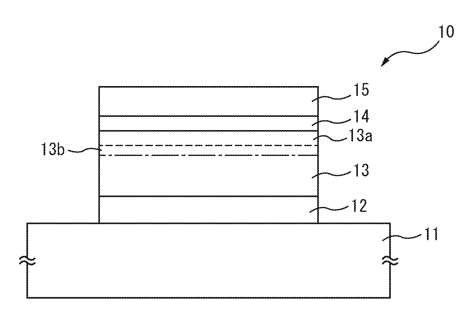
[0092]The thin-film solar cell disclosed in the present specification will be further described below by way of working examples thereof. However, the scope of the present invention is not restricted thereto.

[0093]The thin-film solar cell of Example 1 was produced as described below. As the substrate 11, a glass substrate was used. The first electrode layer 12 was formed by a sputtering method using Mo.

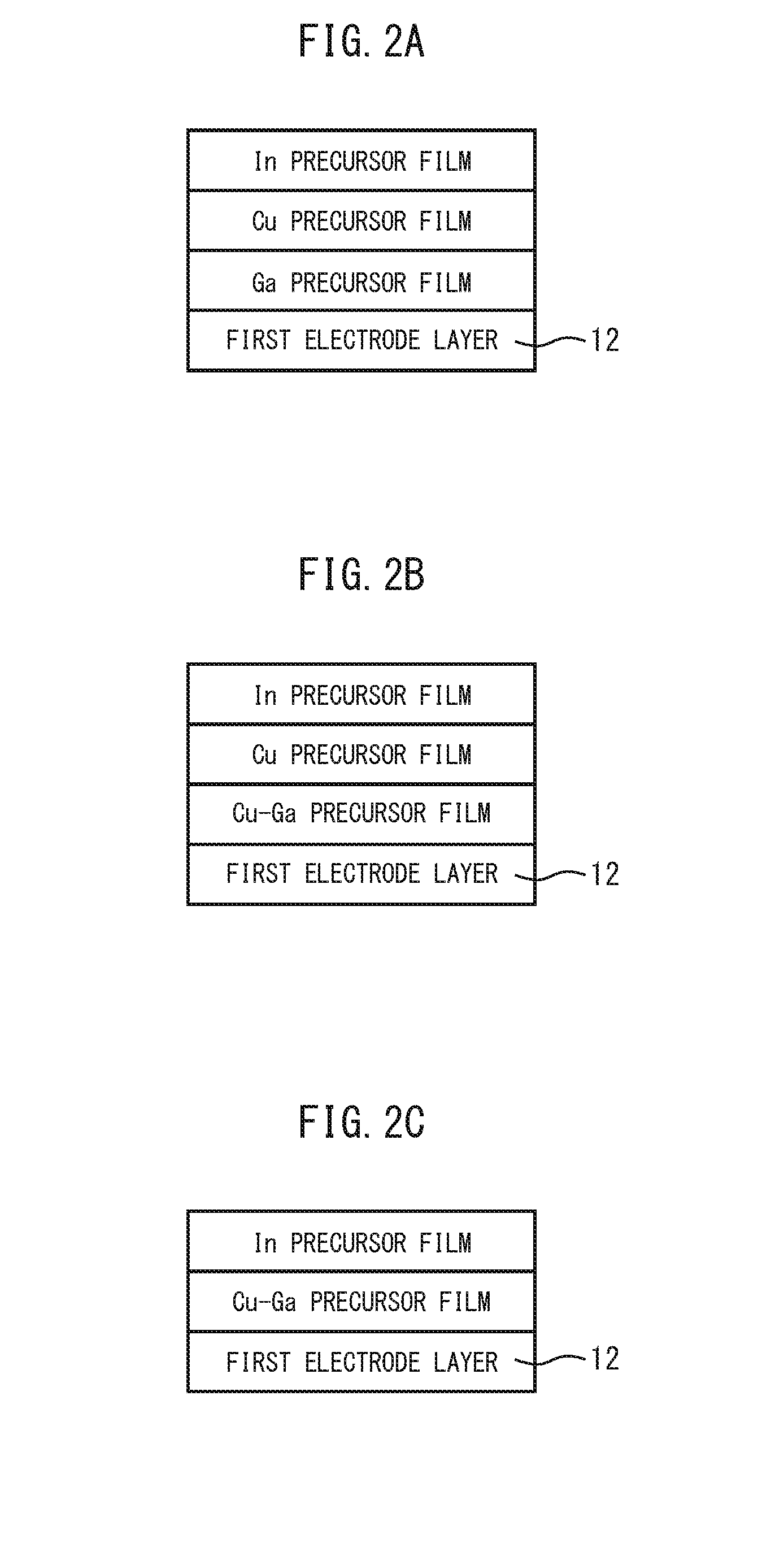
[0094]The p-type light absorption layer 13 was formed by the above-described method (1). As a Group I element, Cu was used. As Group III elements, Ga and In were used and, as Group VI elements, Se and S were used. The p-type light absorption layer 13 was prepared by forming, as precursor films on the first electrode layer, first a CuGa film by a sputtering method, next a Cu film by a sputtering method and then an In film by a sputtering method. The resulting laminate of the thus formed precursor films was subjected to selenization and sulfurization. The buffer layer 14 was formed by a...


PUM

PropertyMeasurementUnit
Fractionaaaaaaaaaa
Thicknessaaaaaaaaaa
Atomic numberaaaaaaaaaa

Abstract

A thin-film solar cell comprising a substrate, a first electrode layer arranged upon the substrate, a p-type light absorption layer formed by a group I-III-IV2 compound arranged upon the first electrode layer, and an n-type second electrode layer arranged upon the p-type light absorption layer. The p-type light absorption layer includes Cu as a group 1 element and includes Ga and In as group III elements. The ratio of the atomic number between Cu and the group III elements in the entire p-type light absorption layer is lower than 1.0; the ratio of the atomic number between Ga and the group III elements in the surface on the second electrode layer side is no more than 0.13; and the ratio of the atomic number between Cu and the group III elements in the surface on the second electrode layer side is at least 1.0.

Description

CROSS-REFERENCE TO RELATED APPLICATIONS[0001]This application is a national stage application under 35 U.S.C. 371 of International Application No. PCT / JP2014 / 066310, filed Jun. 19, 2014, and which claims priority to Japanese Patent Application No. 2013-147092, filed Jul. 12, 2013, the contents of which are incorporated herein by reference in their entirety.FIELD OF THE INVENTION[0002]The present invention relates to a thin-film solar cell and a method of producing the same.BACKGROUND OF THE INVENTION[0003]Conventionally, CIS-based thin-film solar cells which utilize, as a p-type light absorption layer, a Group I-III-VI2 compound semiconductor that has a chalcopyrite structure containing Cu, In, Ga, Se and S have been proposed. Solar cells of this type are relatively inexpensive in terms of production cost and have a high absorption coefficient in the visible to near-infrared wavelength range; therefore, such solar cells are expected to exhibit high photoelectric conversion efficienc...

Claims


Application Information

Patent Timeline
IPC IPC(8): H01L31/0749H01L31/18
CPCH01L31/18H01L31/0749C23C14/185C23C14/5866H01L21/02568H01L21/02614H01L31/0322H01L31/03923H01L31/03928H01L31/065Y02E10/541Y02P70/50C23C28/32
Inventor IWATA, YASUAKISUGIMOTO, HIROKIHAKUMA, HIDEKI
Owner SOLAR FRONTIER
Why Eureka
Try Eureka