

Photoelectric conversion device and method for manufacturing the same
- Summary
- Abstract
- Description
- Claims
- Application Information
AI Technical Summary
Benefits of technology
Problems solved by technology
Method used
Image

Examples
first embodiment
A: First Embodiment
Structure of Photoelectric Conversion Device 100
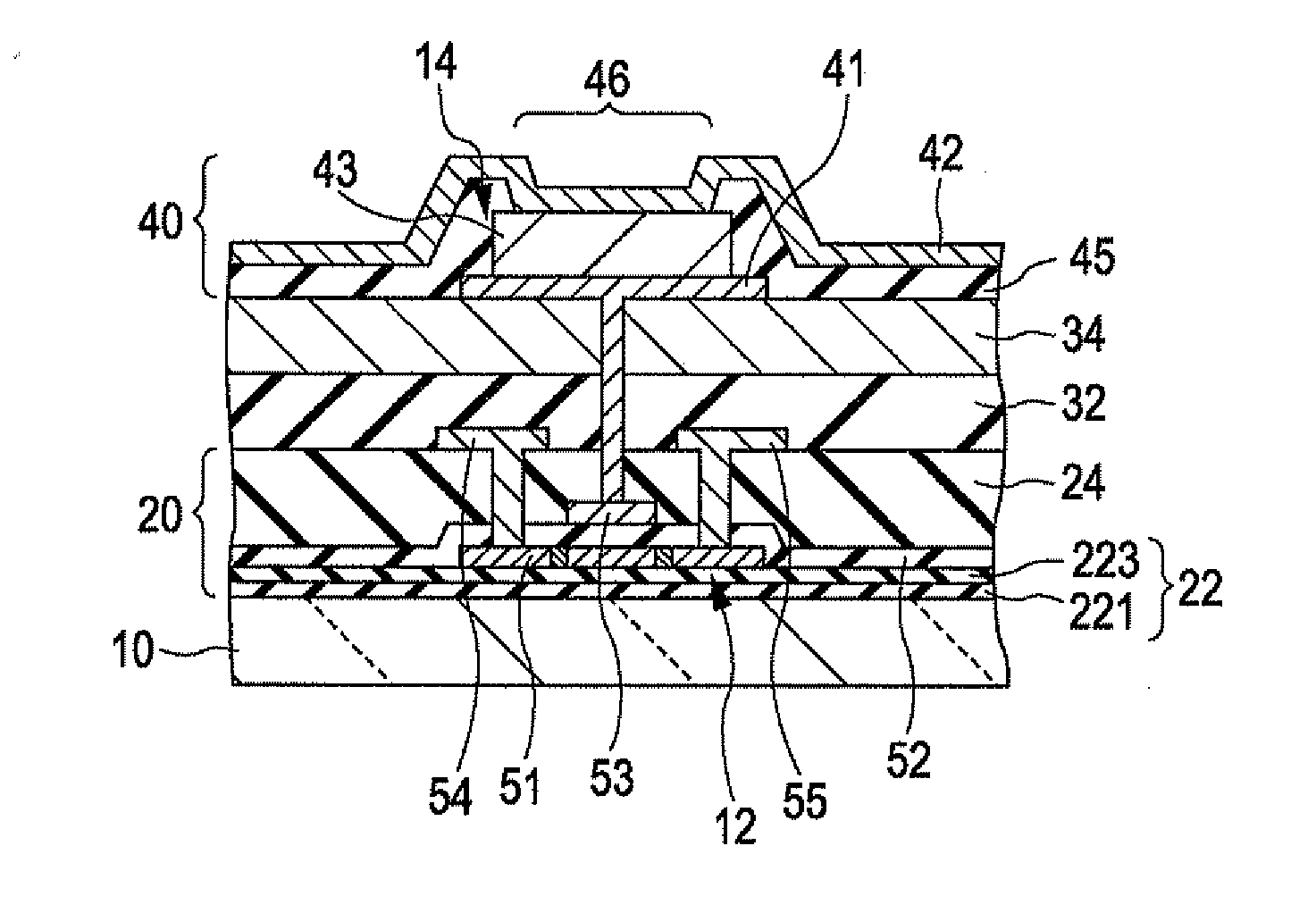
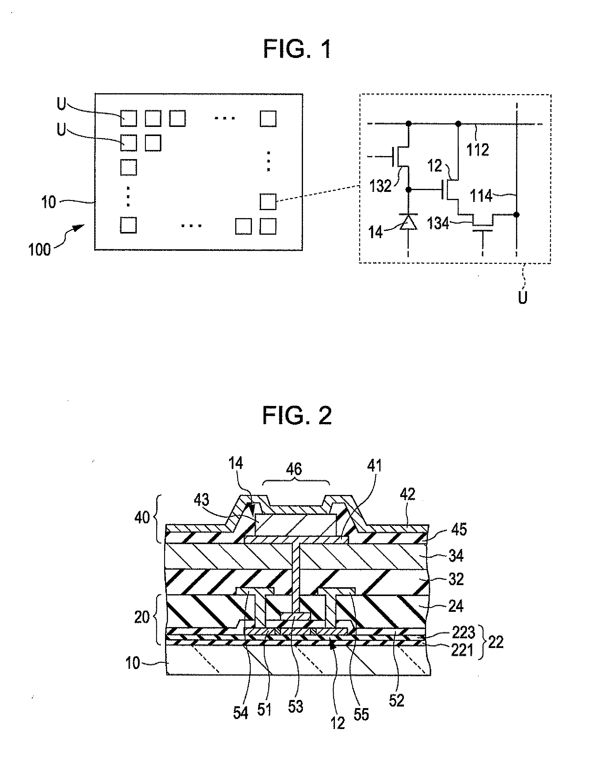
[0017]FIG. 1 is a schematic view of a photoelectric conversion device 100 according to a first embodiment of the invention. The photoelectric conversion device 100 is an imaging device (intravenous sensor) which takes an intravenous image of a living body, for example, for attestation processing, and as shown in FIG. 1, this photoelectric conversion device 100 includes a substrate 10 and a plurality of unit elements U. The substrate 10 is a plate-shaped member, such as a glass substrate. The unit elements U are arranged in a matrix on one surface of the substrate 10.
[0018]As typically shown in FIG. 1, one unit element U is disposed at a position corresponding to the intersection between a constant potential line 112 and a detection line 114 and includes a transistor 12, a transistor 132, a transistor 134, and a photoelectric conversion element 14. The photoelectric conversion element 14 generates a charge correspondi...
second embodiment
B: Second Embodiment
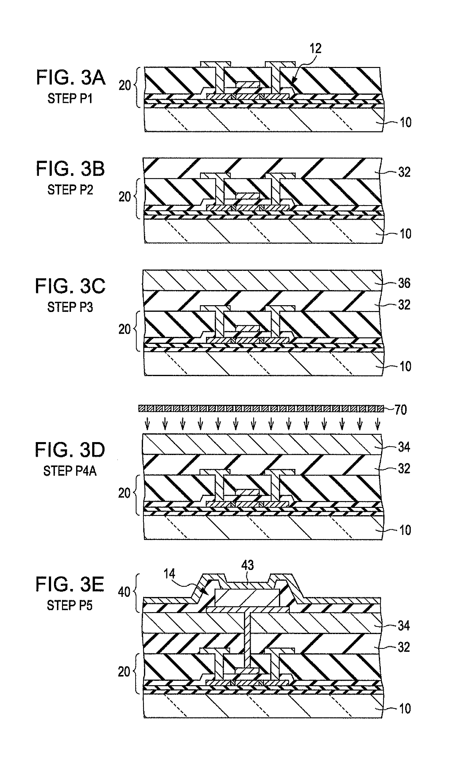
[0038]A second embodiment of the invention will be described. In the second embodiment, instead of using the step P4A of the first embodiment, a step P4B shown in FIG. 5 is performed. As shown in FIG. 5, in the step P4B, the Ia group element is diffused to the base layer 36 formed in the step P3 by a plasma treatment which generates plasma while a mixed gas of an inert carrier gas (such as hydrogen, helium, or argon) and the Ia group element is sprayed to the substrate 10. The concentration of the Ia group element in the mixed gas is selected so that the diffuse density of the Ia group element to the supply layer 34 is approximately 1×10¹⁰ to 1×1016 cm−2 (preferably 1×1012 cm−2)as in the case of the first embodiment.
[0039]An effect similar to that of the first embodiment can also be realized in the second embodiment. In addition, in the second embodiment, since the mixed gas containing the Ia group element is used for the plasma treatment, compared to the case of...
modification 1
1. Modification 1
[0041]The material of the protective layer 32 is not limited to a silicon nitride (SiNx). That is, an optional material which can prevent the diffusion of the Ia group element may be used to form the protective layer 32. As is the case described above, a material of the supply layer 34 is not limited to a silicon oxide (SiOx). For example, the supply layer 34 can be formed using an alkali compound, such as Na3AlF6 disclosed in JP-A-2005-086167. However, a silicon oxide is preferable as the material of the supply layer 34 in view of the handling easiness in a manufacturing process described above. In addition, when the protective layer 32 is formed using a silicon nitride, a silicon oxide is particularly preferable as the material of the supply layer 34 also in view of the adhesion to the protective layer 32 described above.
PUM
 Abstract
Description
Claims
Application Information