Light receiving/emitting element and sensor device using same

Inactive Publication Date: 2016-06-16
KYOCERA CORP
View PDF3 Cites 5 Cited by
  • Summary
  • Abstract
  • Description
  • Claims
  • Application Information

AI Technical Summary

Benefits of technology

[0079]Although the practical exemplary embodiments of the present invention have been described above, the present invention is not limited to the above embodiments, and the present invention can be variously modified within the scope not departing from the gist of the invention.
[0080]As in a first modification illustrated in FIG. 4, for example, the light receiving/emitting element 1 may further include a plurality of lenses 40 that are disposed corresponding to the plurality of light emitting elements 3a, and that condense the lights emitted from the plurality of light emitting elements 3a, respectively. The plurality of lenses 40 are arranged above the corresponding light emitting elements 3a in the direction of thickness of the substrate 2 (i.e., the direction in which the plurality of semiconductor layers are laminated). With such an arrangement, the lights emitted from the light emitting elements 3a are condensed, and a quantity of light incident on the first light receiving element 3b is increased. Hence detection sensitivity of the first light receiving element 3b is increased.
[0081]A plano-convex lens is used as each of the lenses 40 in this modification. Thus, in the lens 40 used in this modification, one principal surface has a convex shape, and the other principal surface has a planar shape. Moreover, a cross-sectional area of the lens 40 is gradually reduced toward the one principal surface from the other principal surface. A material of the lens 40 is optionally selected from not only plastics including thermosetting resins, such as silicone, urethane, and epoxy, and thermoplastic resins, such as polycarbonate and acryl, but also sapphire and inorganic glass. While a plano-convex lens is used as the lens 40 in this embodiment, another type lens, e.g., a biconvex lens may also be used.
[0082]As in a second modification illustrated in FIG. 5, axes of the lights emitted from the plurality of light emitting elements 3a and applied through the plurality of lenses 40, respectively, may be inclined toward the side where the first light receiving element 3b is positioned. In the second modification, the respective axes of the lights emitted from the plurality of light emitting elements 3a are inclined toward the side where the first light receiving element 3b is positioned, by inclining the plurality of

Problems solved by technology

In the above-mentioned type of sensor device, however, because the light receiving element and the light emitting element are independent of each other, problems arise in that productivity is poor d

Method used


Image

  • Light receiving/emitting element and sensor device using same
  • Light receiving/emitting element and sensor device using same
  • Light receiving/emitting element and sensor device using same

Examples


example 1

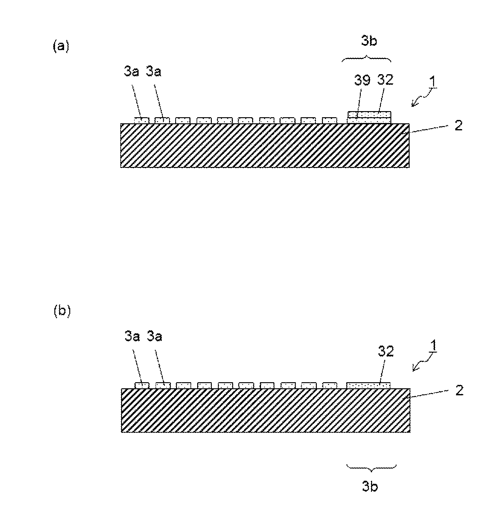
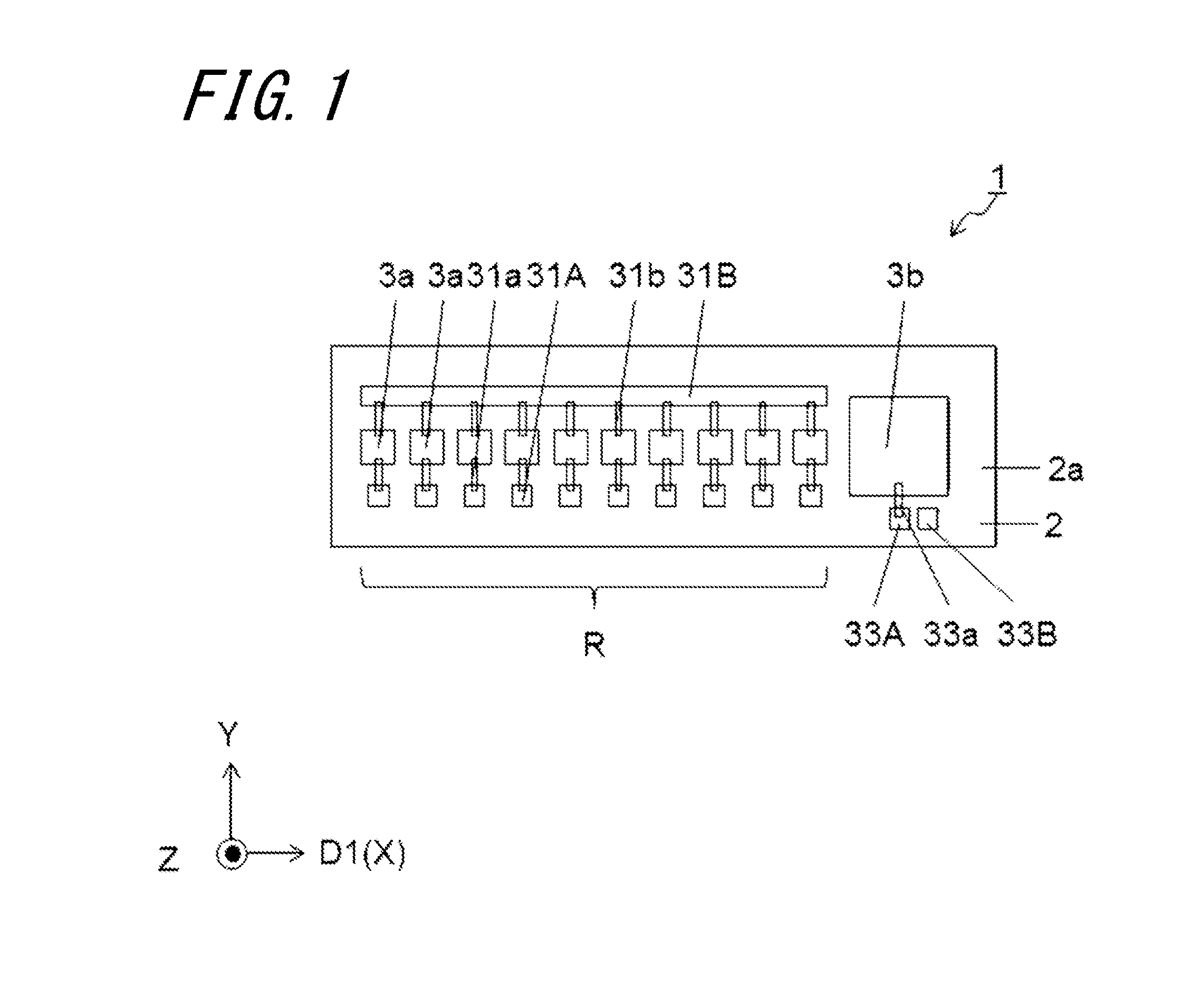
[0094]By using, as a base model, the light receiving / emitting element 1 illustrated in FIG. 1, changes in quantities of the lights received by the first light receiving element 3b were checked by simulation, as detailed below, when the distance to the irradiation target was changed. In the light receiving / emitting element 1, eight light emitting elements 3a were arrayed and successively denoted by 3a1, 3a2, . . . , 3a8 in order starting from the side closest to the first light receiving element 3b. Furthermore, the first direction was defined as an X-direction, and an XY plane parallel to a principal surface of the substrate 2 was defined by the X-direction and a Y-direction perpendicular to the X-direction. A direction normal to the XY plane was defined as a Z-direction.

[0095]First, in the light receiving / emitting element 1, relative positions of the individual light emitting elements 3a and the first light receiving element 3b were determined corresponding to distances (reference ...


PUM


Abstract

A light receiving/emitting element includes a substrate, a plurality of light emitting elements on or in a first surface of the substrate, and a first light receiving element that is a photodiode at the first surface side of the substrate. The plurality of light emitting elements are arranged in a first direction and constitute a light emitting element array, and the first light receiving element is arranged at the one end side of the light emitting element array. The substrate and the plurality of light emitting elements are formed integrally with each other, and the substrate and the first light receiving element are formed integrally with each other. With those features, a light receiving/emitting element and a sensor device can be realized which are small in size, and which have high sensing performance and high response speed.

Description

TECHNICAL FIELD[0001]The present invention relates to a light receiving / emitting element that includes a light receiving element and a light emitting element on the same substrate, and further relates to a sensor device using the light receiving / emitting element.BACKGROUND ART[0002]Various sensor devices have been proposed so far in relation to the type in which light is applied to an irradiation target from a light emitting element and characteristics of the irradiation target are detected by receiving light, which is reflected by the irradiation target upon incidence of the applied light to it, with a light receiving element. Those sensor devices are utilized in a wide field and are used in a variety of applications including, e.g., a photo-interrupter, a photo-coupler, a remote control unit, an IrDA (Infrared Data Association) communication device, an optical fiber communication device, and a document size sensor.[0003]As one example of those sensor devices, Japanese Unexamined P...

Claims


Application Information

Patent Timeline
IPC IPC(8): H01L31/12H01L33/58
CPCH01L33/58H01L31/125H01L31/173H01L25/0753H01L25/167
Inventor OKUSHIBA, HIROYUKI
Owner KYOCERA CORP
Why Eureka
Try Eureka