
Lvds with idle state

a technology of idle state and lvd, which is applied in the direction of pulse generator, logic circuit coupling/interface arrangement, pulse technique, etc., can solve the problem of indeterminate output of common mode feedback amplifier

Active Publication Date: 2016-06-16
NXP USA INC
View PDF0 Cites 0 Cited by
  • Summary
  • Abstract
  • Description
  • Claims
  • Application Information

AI Technical Summary

Benefits of technology

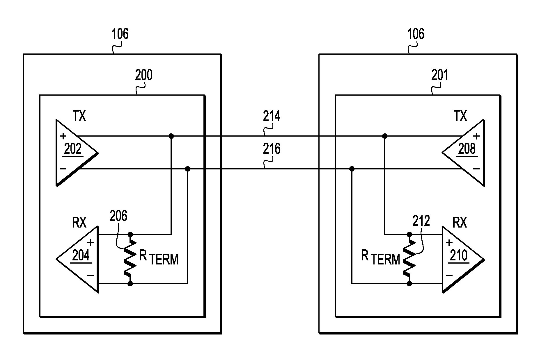
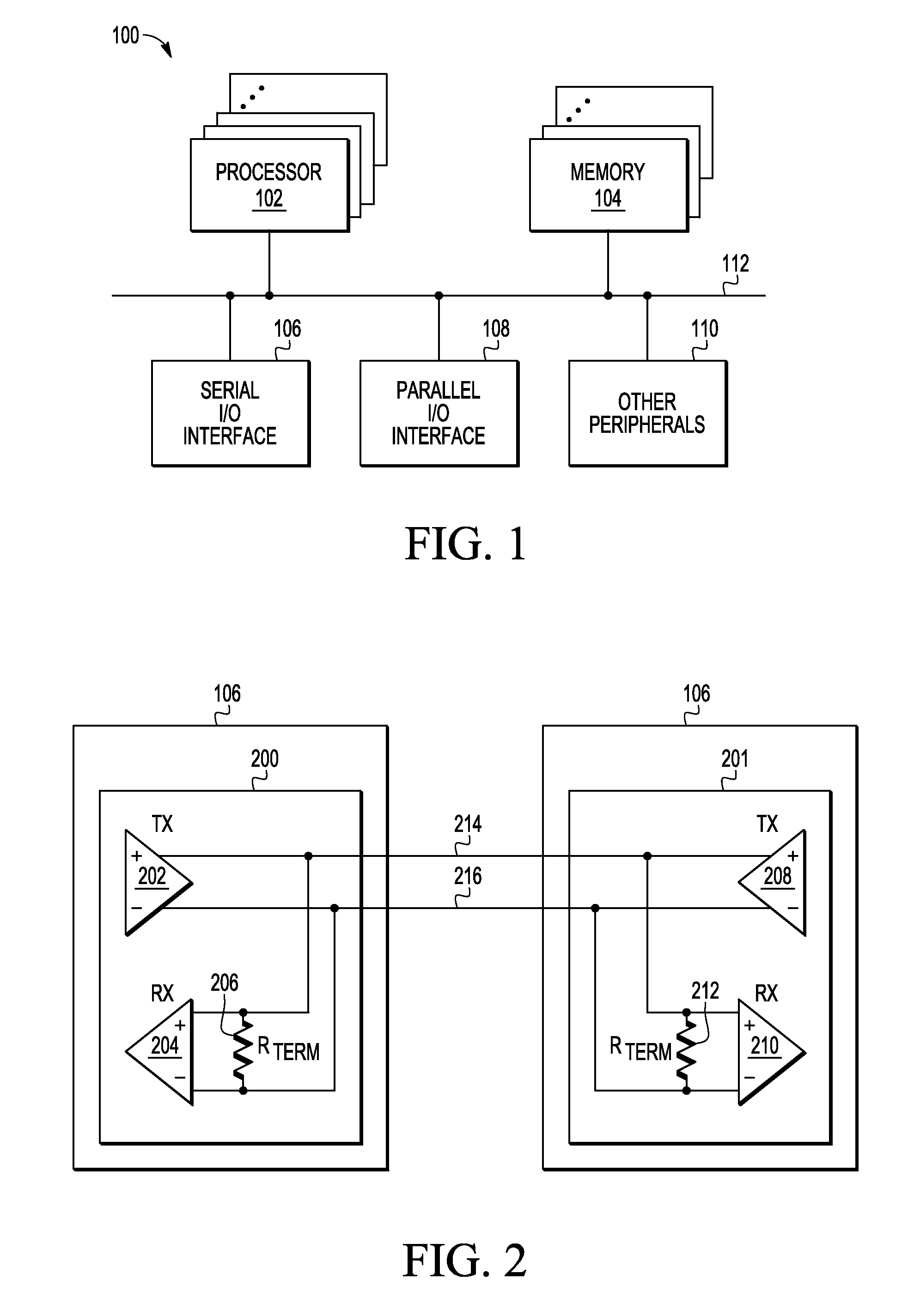
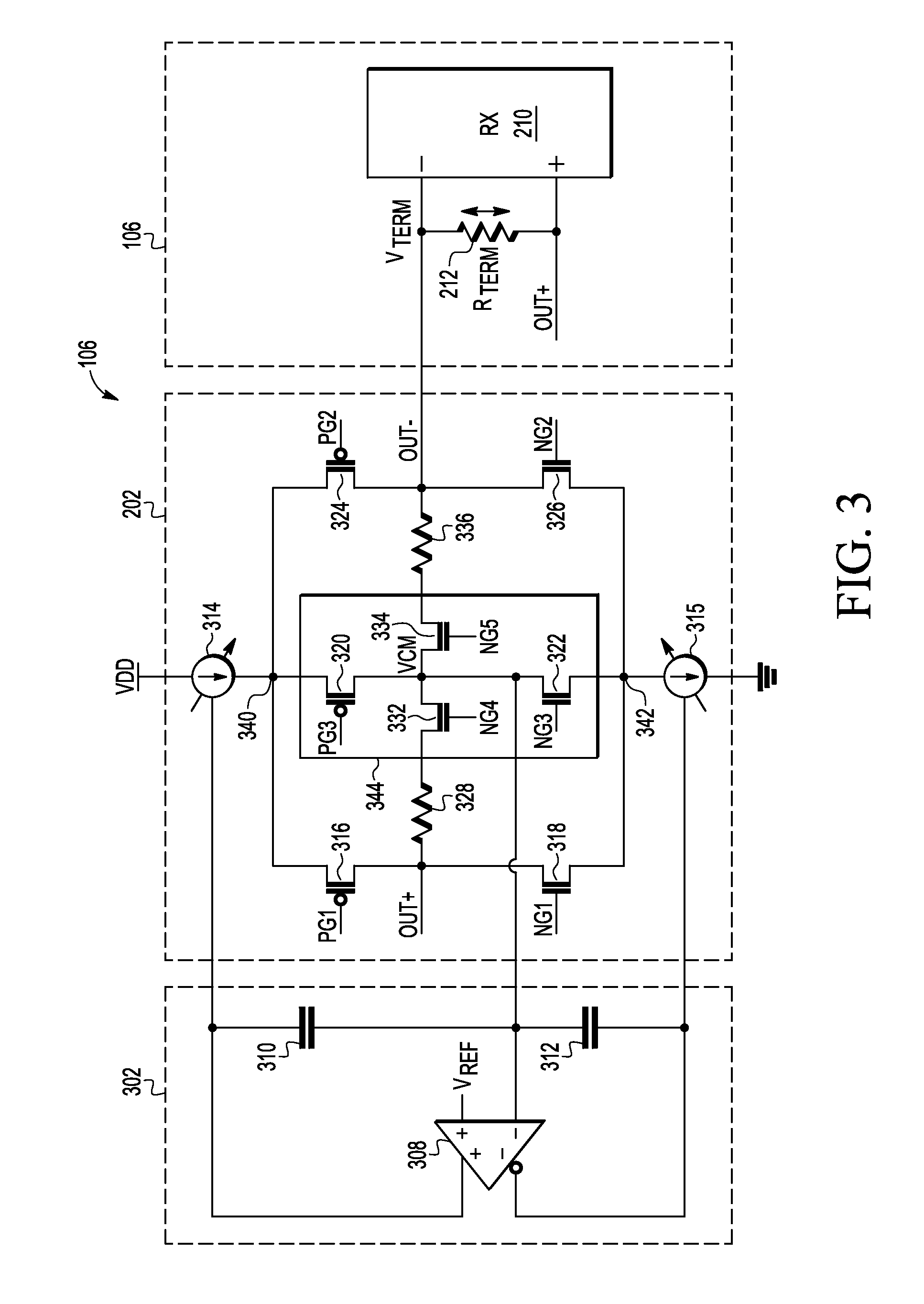
This patent describes a system and method for a low voltage signaling (LVDS) transmitter that has a standby or idle current path. This allows the transmitter to enter a standby mode when using common lines to transmit and receive data between devices. In standby mode, the transmitter can still operate normally while being isolated from the data path. This standby current path also allows the output to be in a high impedance state for receiver functionality. By maintaining the transmitter in standby mode during receiver operation, startup delay of the transmitter when switching back to transmit mode is sharply reduced. This circuit topology of the transmitter can be used in multiple LVDS applications and can be implemented in any semiconductor technology process node.

Problems solved by technology

In a traditional LVDS circuit, disabling the output devices removes the common mode voltage, which in turn causes the output of the common mode feedback amplifier to be indeterminate.

Method used


Image

  • Lvds with idle state
  • Lvds with idle state
  • Lvds with idle state

Examples


Embodiment Construction

[0010]Embodiments of systems, devices and methods are disclosed for a low voltage signaling (LVDS) transmitter with a standby or idle current path in the output switching stage of the LVDS circuit. When common lines are used to transmit and receive data between devices, the transmitter does not need to be fully shut down during receive mode, but rather can enter the idle or standby mode. The standby current path maintains voltage at a common mode feedback amplifier during the idle mode, and allows the current sources and feedback amplifier to operate normally while being isolated from the data path of the transmitter. The standby current path further allows the output to be in a high impedance state for receiver functionality. Maintaining the transmitter in standby mode during receiver operation sharply reduces startup delay of the transmitter when switching back to transmit mode. For example, by allowing the transmitter to remain in standby mode, the time required to switch from re...


PUM


Abstract

A low voltage differential signaling generating circuit, which comprises a current source a pair of output nodes for providing a differential signal by virtue of a voltage difference therebetween, first and second differential switch circuitries and a bypass circuitry. The first differential switch circuitry selectively connects the current source to the first output node based on a control signal to cause a current flow from the first output node to the second one. The second differential switch circuitry selectively connects the current source to the second output node based on the control signal to cause a current flow from the second output node to the first one. The bypass circuitry is arranged in parallel to the first and second differential switch circuitries and is selectively switched based on an idle mode signal to prevent a current between the output nodes.

Description

BACKGROUND[0001]1. Field[0002]This disclosure relates generally to semiconductor devices, and more specifically, to low voltage differential signaling transmitter capable of operating in a standby state.[0003]2. Related Art[0004]Start-up time for a traditional Low Voltage Differential Signaling (LVDS) circuit is dominated by the settling time of a common mode feedback amplifier. In a traditional LVDS circuit, disabling the output devices removes the common mode voltage, which in turn causes the output of the common mode feedback amplifier to be indeterminate. The time required to re-establish a stable common mode voltage after enabling of the output devices ultimately defines the startup time, which is normally much longer than the standard data transmit time. For example, the settling time of the amplifier may be approximately 500 nanoseconds, but a specification for the LVDS may require the device to be capable of operating within a much shorter time frame, such as 7 nanoseconds a...

Claims


Application Information

Patent Timeline
Patent Type & Authority Applications(United States)
IPC IPC(8): H03K19/0175H03K3/012
CPCH03K3/012H03K19/0175H03K19/017509H04L25/0272
Inventor PHILLIPPE, JONATHAN M.LUBBERS, GILFORD E.MICIELLI, CHRIS J.
Owner NXP USA INC
Learn More