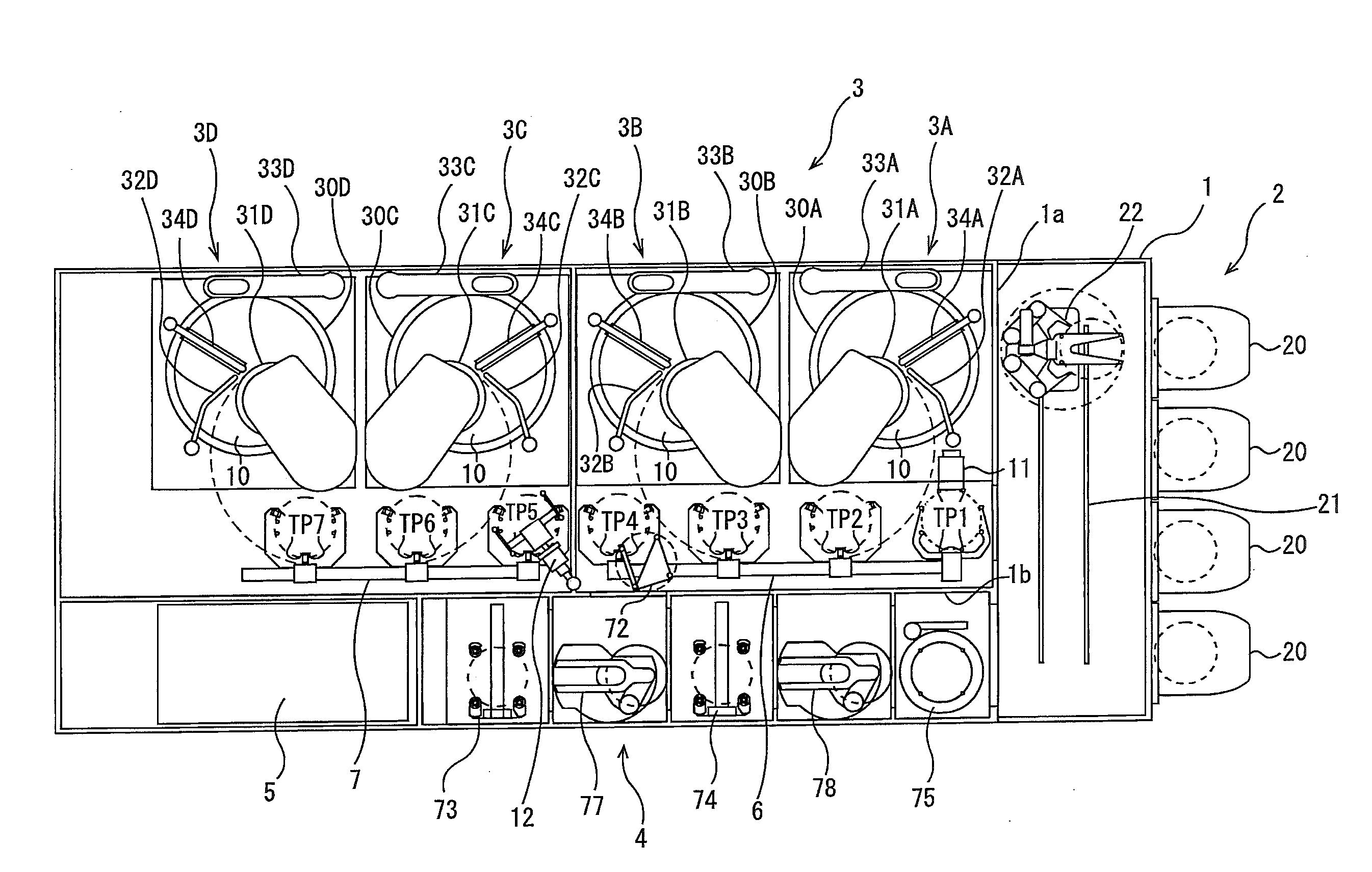
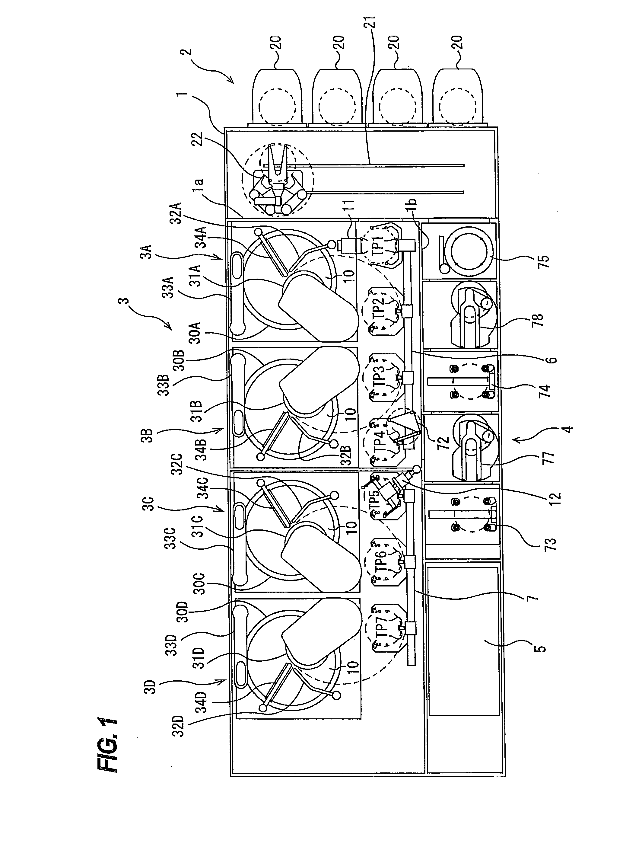
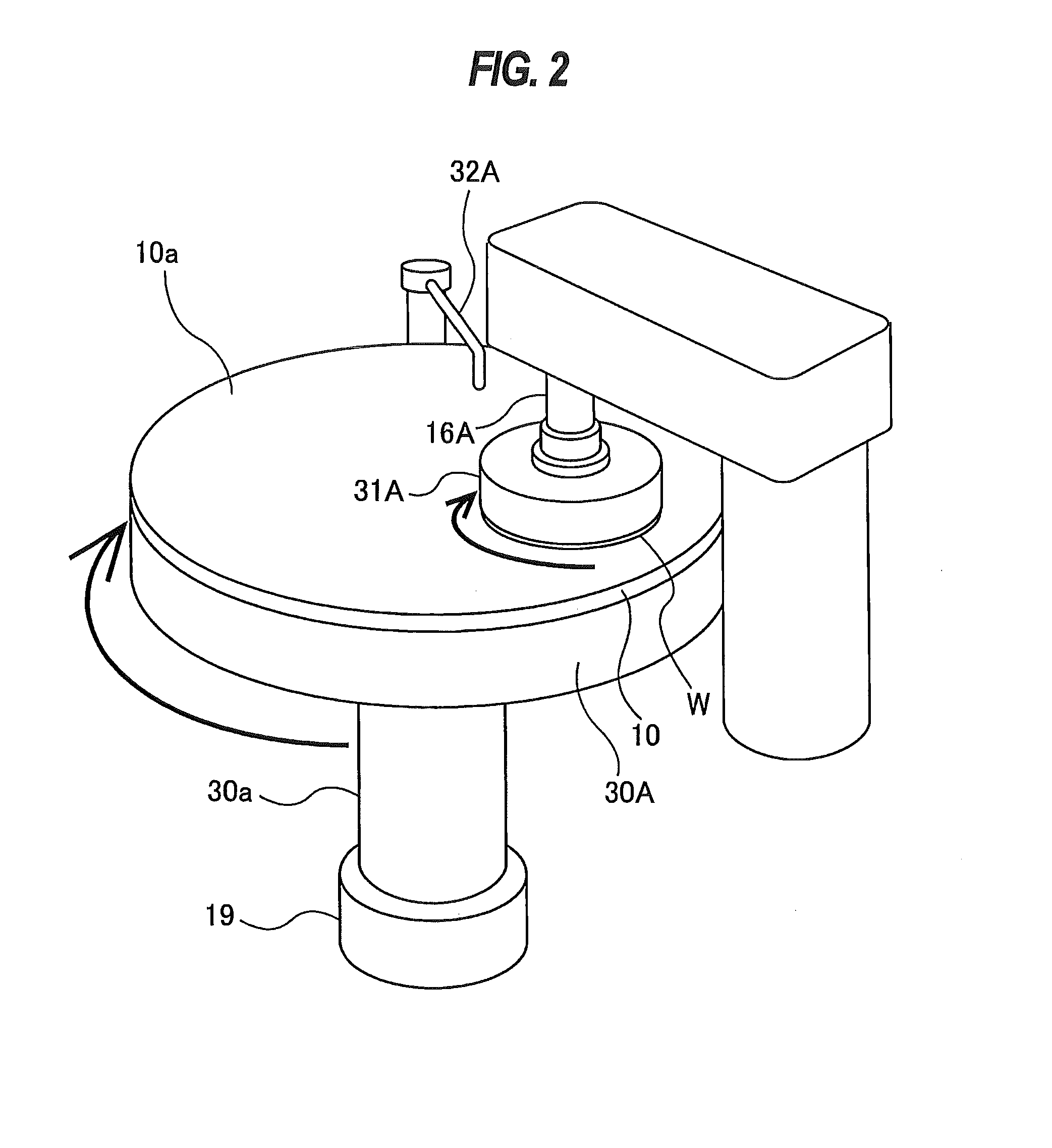
Polishing apparatus

a technology of polishing apparatus and rotary blade, which is applied in the direction of lapping machines, manufacturing tools, transportation and packaging, etc., can solve the problems of increasing maintenance costs and running costs, poor film formation (or step coverage) over stepped configurations of thin films, and reducing the operation rate of the apparatus

Inactive Publication Date: 2016-06-23
EBARA CORP
View PDF14 Cites 0 Cited by
  • Summary
  • Abstract
  • Description
  • Claims
  • Application Information

AI Technical Summary

Benefits of technology

[0012]According to an embodiment, there is provided a low-cost polishing apparatus which can perform multistage polishing of a substrate, such as a wafer.
[0013]According to embodiments, there are provided a polishing apparatus and a polishing method which can more precisely control a profile of a substrate, such as a wafer.
[0014]Further, according to an embodiment, there is provided a polishing apparatus provided with different types of polishing heads which can perform optimum multistage polishing under different polishing conditions.
[0024]According to the above-described embodiments, the plurality of polishing heads having different structures, i.e., having different initial costs and maintenance costs, are used. The use of the plurality of polishing heads having different structures can reduce a frequency of using a polishing head that requires a high maintenance cost. Therefore, the total maintenance cost of the polishing apparatus can be reduced.
[0025]According to the above-described embodiments, the first polishing head and the second polishing head, having the pressure chambers in different arrangements, are used. These two polishing heads can press different areas of a substrate against the polishing pad. In other words, the use of the two polishing heads, having the pressure chambers in different arrangements, can achieve the same effect as that achieved by use of a single polishing head having an increased number of pressure chambers. Therefore, a profile of a substrate can be controlled more precisely.
[0044]The polishing apparatus according to the above-described embodiments can perform optimum multistage polishing with use of the different types of polishing heads. For example, a wafer is polished at a relatively high pressure with use of a polishing head having a high-hardness elastic membrane in the first-stage polishing, and the wafer is polished at a relatively low pressure with use of a polishing head having a low-hardness elastic membrane in the second-stage polishing. In another exemplary process, in order to obtain different wafer-edge profiles in the first-stage polishing and the second-stage polishing, the first-stage polishing and the second-stage polishing are performed using polishing heads whose elastic membranes have different shapes of edge portions. It is also possible to use a high-hardness polishing pad in the first-stage polishing and to use, in the second-stage polishing, a polishing head whose retainer ring has the smaller number of grooves than the retainer ring used in the first-stage polishing or has a tapered or oval edge portion. A width of a retainer ring affects rebound characteristics of a polishing pad and a flow of a polishing liquid being supplied to a wafer surface. Therefore, two polishing heads, provided with retainer rings having different widths, may be used to perform multistage polishing of a wafer.

Problems solved by technology

An increase in the number of interconnect layers would result in poor film formation (or step coverage) over stepped configurations of thin films.
Furthermore, miniaturization of a photolithographic process necessitates a smaller depth of focus in a photolithographic optical system, and therefore a surface of the semiconductor device needs to be planarized such that the irregularities or steps on the surface of the semiconductor device will fall within the depth of focus.
However, such a high-performance polishing head has a complicated structure and has costly consumables (the membrane, the retainer ring, etc.), and therefore entails an increased maintenance cost and an increased running cost.
Further, a frequency of maintenance work will also increase, resulting in a decrease in an operation rate of the apparatus.
However, the polishing head of this type cannot control the polishing rate in smaller areas than the pressure chambers.
It is possible to perform finer control of a wafer profile by using more pressure chambers, but there is a limit on the number of pressure chambers that can be provided in the polishing head.
Furthermore, the above-described polishing head is not able to positively control a polishing rate of a wafer at a boundary between the pressure chambers, and therefore the polishing rate may be low at the boundary between the pressure chambers.

Method used


Image

  • Polishing apparatus
  • Polishing apparatus
  • Polishing apparatus

Examples


example 2

[0129 represents an exemplary selection of polishing heads in a case of a small amount of polishing of a wafer, a high demand for planarization of a wafer surface and a high demand for no defect. In this example 2, the rigid-body polishing head of the first polishing unit 3A is not used, while the second multi-chamber polishing head of the second polishing unit 3B, the second multi-chamber polishing head of the third polishing unit 3C, and the rigid-body polishing head of the fourth polishing unit 3D are used. Example 3 represents an exemplary selection of polishing heads in a case of a small amount of polishing of a wafer, a low demand for planarization of a wafer surface and a high demand for no defect. In this Example 3, the rigid-body polishing head of the first polishing unit 3A and the second multi-chamber polishing head of the third polishing unit 3C are not used, while the second multi-chamber polishing head of the second polishing unit 3B and the rigid-body polishing head o...


PUM

PropertyMeasurementUnit
pressureaaaaaaaaaa
pressureaaaaaaaaaa
thicknessaaaaaaaaaa

Abstract

A polishing apparatus capable of performing multi-stage polishing of a substrate, such as wafer, is disclosed. The polishing apparatus includes: a plurality of polishing tables each for supporting a polishing pad; a plurality of polishing heads each configured to press a substrate against the polishing pad; and a transporting device configured to transport the substrate to at least two of the plurality of polishing heads. The plurality of polishing heads have different structures.

Description

CROSS REFERENCE TO RELATED APPLICATIONS[0001]This document is a Divisional application of U.S. patent Ser. No. 14 / 672,003 filed Mar. 27, 2015, which claims priorities to Japanese Patent Application Number 2014-072965 filed Mar. 31, 2014 and Japanese Patent Application Number 2014-229169 filed Nov. 11, 2014, the entire contents of which are hereby incorporated by reference.BACKGROUND[0002]As semiconductor devices have been in a trend toward high integration and high density in recent years, circuit interconnects are also becoming smaller and finer, and the larger number of layers are used to form multilayer interconnects. The multilayer interconnects with the finer circuits entail greater surface steps which reflect surface irregularities of lower layers. An increase in the number of interconnect layers would result in poor film formation (or step coverage) over stepped configurations of thin films. Therefore, better multilayer interconnects need to have the improved step coverage an...

Claims


Application Information

Patent Timeline
Patent Type & Authority Applications(United States)
IPC IPC(8): B24B37/10H01L21/677H01L21/67B24B37/34
CPCB24B37/10H01L21/67219H01L21/67742B24B37/345B24B37/34H01L21/02024
Inventor YOSHIDA, HIROSHIFUKUSHIMA, MAKOTOYASUDA, HOZUMI
Owner EBARA CORP
Why Eureka
Try Eureka